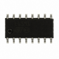
L6591 STMicroelectronics, L6591 Datasheet - Page 6

L6591
Manufacturer Part Number
L6591
Description
IC CTRLR PWM PROG CM HV 16SOIC
Manufacturer
STMicroelectronics
Specifications of L6591
Output Isolation
Isolated
Frequency Range
168 ~ 192kHz
Voltage - Input
8.7 ~ 22 V
Power (watts)
750mW
Operating Temperature
-40°C ~ 150°C
Package / Case
16-SOIC (0.154", 3.90mm Width)
Output Voltage
5 V
Input Voltage
25 V
Operating Temperature Range
- 40 C to + 150 C
Mounting Style
SMD/SMT
Duty Cycle (max)
50 %
For Use With
497-8335 - BOARD EVAL FOR L6591
Lead Free Status / RoHS Status
Lead free / RoHS Compliant
Other names
497-8286
Available stocks
Company
Part Number
Manufacturer
Quantity
Price
Part Number:
L6591
Manufacturer:
ST
Quantity:
20 000
Part Number:
L6591TR
Manufacturer:
ST
Quantity:
20 000
Pin settings
6/41
Table 1.
Pin N.
10
11
12
13
14
15
16
9
HVSTART
Pin functions (continued)
FGND
BOOT
Name
GND
HVG
N.C.
LVG
Vcc
Supply voltage of both the signal part of the IC and the low-side gate driver.
The internal high voltage generator charges an electrolytic capacitor
connected between this pin and GND (#11) as long as the voltage on the
pin is below the start-up threshold of the IC, after that it is disabled and the
chip turns on. Sometimes a small bypass capacitor (0.1 µF typ.) to GND
might be useful to get a clean bias voltage for the signal part of the IC. The
minimum operating voltage (UVLO) is adapted to the loading conditions of
the converter to ease burst-mode operation, during which the available
supply voltage for the IC drops.
Low-side gate-drive output. The driver is capable of 0.3 A min. source and
0.8 A min. sink peak current to drive the gate of the lower MOSFET of the
half-bridge leg. The pin is actively pulled to GND (#11) during UVLO.
Chip ground. Current return for both the low-side gate-drive current and the
bias current of the IC. All of the ground connections of the bias components
should be tied to a track going to this pin and kept separate from any pulsed
current return.
High-voltage spacer. The pin is not connected internally to isolate the group
of high-voltage pins and comply with safety regulations (creepage distance)
on the PCB.
High-side gate-drive floating ground. Current return for the high-side gate-
drive current. Layout carefully the connection of this pin to avoid too large
spikes below ground.
High-side floating gate-drive output. The driver is capable of 0.3 A min.
source and 0.8 A min. sink peak current to drive the gate of the upper
MOSFET of the half-bridge leg. A pull-down resistor between this pin and
pin 13 (FGND) makes sure that the gate is never floating during UVLO.
High-side gate-drive floating supply voltage. The bootstrap capacitor
connected between this pin and pin 13 (FGND) is fed by an internal
synchronous bootstrap diode driven in-phase with the low-side gate-drive.
This patented structure can replace the normally used external diode.
High-voltage start-up. The pin is to be connected directly to the rectified
mains voltage. A 0.8 mA internal current source charges the capacitor
connected between pin Vcc (#9) and GND (#11) until the voltage on the Vcc
pin reaches the start-up threshold. Normally it is re-enabled when the
voltage on the Vcc pin falls below 5 V, except under latched shutdown
conditions, in which case it is re-enabled as the Vcc voltage falls 1 V below
the start-up threshold to keep the latch active.
Doc ID 14821 Rev 5
Function
L6591


