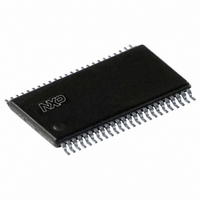
PCF8562TT/2,118 NXP Semiconductors, PCF8562TT/2,118 Datasheet - Page 18

PCF8562TT/2,118
Manufacturer Part Number
PCF8562TT/2,118
Description
IC LCD DRIVER 32/128SEG 48-TSSOP
Manufacturer
NXP Semiconductors
Datasheet
1.PCF8562TT2118.pdf
(37 pages)
Specifications of PCF8562TT/2,118
Package / Case
48-TSSOP
Display Type
LCD
Configuration
7 Segment + DP, 14 Segment (32 Segment)
Interface
I²C
Current - Supply
32µA
Voltage - Supply
1.8 V ~ 5.5 V
Operating Temperature
-40°C ~ 85°C
Mounting Type
Surface Mount
Number Of Digits
16
Number Of Segments
32
Maximum Clock Frequency
2640 Hz
Operating Supply Voltage
1.8 V to 5.5 V
Maximum Power Dissipation
400 mW
Maximum Operating Temperature
+ 85 C
Attached Touch Screen
No
Maximum Supply Current
20 uA
Minimum Operating Temperature
- 40 C
Lead Free Status / RoHS Status
Lead free / RoHS Compliant
For Use With
OM6292 - DEMO BOARD PCA2125 RTCOM10088 - KIT FOR LCD DEMO LPC900622-1003 - KIT FOR LCD DEMO
Digits Or Characters
-
Lead Free Status / Rohs Status
Lead free / RoHS Compliant
Other names
568-2029-2
PCF8562TT/2,518
PCF8562TT/2-T
PCF8562TT/2,518
PCF8562TT/2-T
NXP Semiconductors
PCF8562_5
Product data sheet
7.14 Input bank selector
7.15 Blinker
the contents of rows 2 and 3 may be selected instead of rows 0 and 1. This gives the
provision for preparing display information in an alternative bank and to be able to switch
to it once it is assembled.
The input bank selector loads display data into the display RAM in accordance with the
selected LCD drive configuration.
The bank-select command (see
static drive mode or in rows 2 and 3 in 1:2 mode. The input bank selector functions are
independent of the output bank selector.
The PCF8562 has a very versatile display blinking capability. The whole display can blink
at a frequency selected by the blink-select command (see
is a fraction of the clock frequency; the ratio between the clock frequency and blink
frequency depends on the blink mode selected (see
An additional feature allows an arbitrary selection of LCD segments to blink in the static
and 1:2 drive modes. This is implemented without any communication overheads by the
output bank selector which alternates the displayed data between the data in the display
RAM bank and the data in an alternative RAM bank at the blink frequency. This mode can
also be implemented by the blink-select command (see
In the 1:3 and 1:4 drive modes, where no alternative RAM bank is available, groups of
LCD segments can blink selectively by changing the display RAM data at fixed time
intervals.
The entire display can blink at a frequency other than the nominal blink frequency by
sequentially resetting and setting the display enable bit E at the required rate using the
mode-set command (see
Table 6.
[1]
Blink mode
off
1
2
3
Blink modes 1, 2 and 3 and the nominal blink frequencies 0.5 Hz, 1 Hz and 2 Hz correspond to an oscillator
frequency (f
Blinking frequencies
clk
) of 1536 Hz (see
All information provided in this document is subject to legal disclaimers.
Rev. 05 — 19 May 2010
Section
Normal operating mode ratio
-
--------- -
768
------------ -
1536
------------ -
3072
f
f
f
clk
clk
clk
Section
[1]
Section
7.17).
11).
7.17) can be used to load display data in row 2 in
Universal LCD driver for low multiplex rates
Table
Section
Table
6).
Nominal blink frequency
blinking off
2 Hz
1 Hz
0.5 Hz
13). Each blink frequency
7.17).
PCF8562
© NXP B.V. 2010. All rights reserved.
18 of 37


