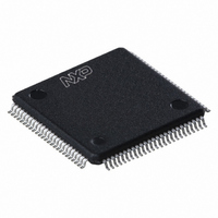
PCF2113DH/4,557 NXP Semiconductors, PCF2113DH/4,557 Datasheet - Page 12

PCF2113DH/4,557
Manufacturer Part Number
PCF2113DH/4,557
Description
IC LCD CONTROLLER/DRIVER 100LQFP
Manufacturer
NXP Semiconductors
Datasheet
1.PCF2113DH4557.pdf
(65 pages)
Specifications of PCF2113DH/4,557
Package / Case
100-LQFP
Display Type
LCD
Configuration
5 X 8 (Matrix)
Interface
I²C
Voltage - Supply
2.2 V ~ 4 V
Operating Temperature
-40°C ~ 85°C
Mounting Type
Surface Mount
Number Of Digits
40
Maximum Clock Frequency
450 KHz
Operating Supply Voltage
1.8 V to 5.5 V
Maximum Power Dissipation
400 mW
Maximum Operating Temperature
+ 75 C
Attached Touch Screen
No
Maximum Supply Current
50 mA
Minimum Operating Temperature
- 20 C
Operating Supply Voltage (typ)
2.5/3.3/5V
Package Type
LQFP
Pin Count
100
Mounting
Surface Mount
Power Dissipation
400mW
Operating Supply Voltage (min)
1.8V
Operating Supply Voltage (max)
5.5V
Lead Free Status / RoHS Status
Lead free / RoHS Compliant
Current - Supply
-
Digits Or Characters
-
Lead Free Status / Rohs Status
Lead free / RoHS Compliant
Other names
935276328557
PCF2113DH/4
PCF2113DH/4
PCF2113DH/4
PCF2113DH/4
Available stocks
Company
Part Number
Manufacturer
Quantity
Price
Company:
Part Number:
PCF2113DH/4,557
Manufacturer:
NXP Semiconductors
Quantity:
10 000
NXP Semiconductors
PCF2113_FAM_4
Product data sheet
8.8 Address counter
8.9 Display data RAM
The Address Counter (AC) assigns addresses to the DDRAM and CGRAM for reading
and writing and is set by the commands ‘set DDRAM address’ and ‘set CGRAM address’.
After a read/write operation the address counter is automatically incremented or
decremented by 1. The address counter contents are output to the bus (DB6 to DB0)
when bit RS = 0 and bit R/W = 1.
The Display Data RAM (DDRAM) stores up to 80 characters of display data represented
by 8-bit character codes. RAM locations which are not used for storing display data can be
used as general purpose RAM. The basic RAM to display addressing scheme is shown in
Figure
locations starting at address 00h in line 1 are displayed.
display mapping for right and left shift respectively.
When data is written to or read from the DDRAM, wrap-around occurs from the end of one
line to the start of the next line. When the display is shifted each line wraps around within
itself, independently of the others. Thus all lines are shifted and wrapped around together.
The address ranges and wrap-around operations for the various modes are shown in
Table
Fig 4.
Fig 5.
7.
4. With no display shift the characters represented by the codes in the first 24 RAM
DDRAM to display mapping: no shift
DDRAM to display mapping: right shift
display
position
DDRAM
address
1-line display
DDRAM
address
2-line display
00 01 02 03 04
00 01 02 03 04
40 41 42 43 44
1 2 3 4 5
1 2 3 4 5
1 2 3 4 5
Rev. 04 — 4 March 2008
display
position
DDRAM
address
1-line display
DDRAM
address
2-line display
4F 00 01 02 03
27 00 01 02 03
67 40 41 42 43
1 2 3 4 5
1 2 3 4 5
1 2 3 4 5
22 23 24
10 11 12
10 11 12
15 16 17 18 19
09 0A 0B 0C 0D
49 4A 4B 4C 4D
non-displayed DDRAM address
non-displayed DDRAM addresses
22 23 24
10 11 12
10 11 12
14 15 16
08 09 0A
48 49 4A
mge992
Figure 5
line 1
line 2
24 25 26 27
64 65 66 67
LCD controllers/drivers
and
mge991
PCF2113x
4C 4D 4E 4F
Figure 6
© NXP B.V. 2008. All rights reserved.
line 1
line 2
show the
12 of 65


