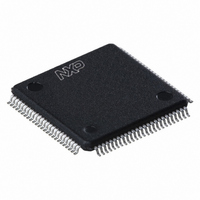
PCF2113DH/4,557 NXP Semiconductors, PCF2113DH/4,557 Datasheet - Page 24

PCF2113DH/4,557
Manufacturer Part Number
PCF2113DH/4,557
Description
IC LCD CONTROLLER/DRIVER 100LQFP
Manufacturer
NXP Semiconductors
Datasheet
1.PCF2113DH4557.pdf
(65 pages)
Specifications of PCF2113DH/4,557
Package / Case
100-LQFP
Display Type
LCD
Configuration
5 X 8 (Matrix)
Interface
I²C
Voltage - Supply
2.2 V ~ 4 V
Operating Temperature
-40°C ~ 85°C
Mounting Type
Surface Mount
Number Of Digits
40
Maximum Clock Frequency
450 KHz
Operating Supply Voltage
1.8 V to 5.5 V
Maximum Power Dissipation
400 mW
Maximum Operating Temperature
+ 75 C
Attached Touch Screen
No
Maximum Supply Current
50 mA
Minimum Operating Temperature
- 20 C
Operating Supply Voltage (typ)
2.5/3.3/5V
Package Type
LQFP
Pin Count
100
Mounting
Surface Mount
Power Dissipation
400mW
Operating Supply Voltage (min)
1.8V
Operating Supply Voltage (max)
5.5V
Lead Free Status / RoHS Status
Lead free / RoHS Compliant
Current - Supply
-
Digits Or Characters
-
Lead Free Status / Rohs Status
Lead free / RoHS Compliant
Other names
935276328557
PCF2113DH/4
PCF2113DH/4
PCF2113DH/4
PCF2113DH/4
Available stocks
Company
Part Number
Manufacturer
Quantity
Price
Company:
Part Number:
PCF2113DH/4,557
Manufacturer:
NXP Semiconductors
Quantity:
10 000
NXP Semiconductors
9. Instructions
Table 9.
[1]
[2]
PCF2113_FAM_4
Product data sheet
I
commands
[1]
2
C-bus
R/W is set together with the slave address.
For explanation, see
Instruction set for I
Control byte
Co
[2]
RS 0
Table
Table 8.
Only two PCF2113x registers, the Instruction Register (IR) and the Data Register (DR),
can be directly controlled by the microcontroller. Before internal operation, control
information is stored temporarily in these registers to allow interfacing to various types of
microcontrollers which operate at different speeds or to allow interfacing to peripheral
control ICs.
The instruction set for I
how these control and command bytes are embedded in the I
The PCF2113x operation is controlled by the instructions shown in
their execution time. Details are explained in subsequent sections.
Step
1
2
3
4
5
6
7
8
9
10
11
11.
0
2
Function
clear display
entry mode set
display control
function set
default address pointer
to DDRAM
icon control
display or screen
configuration
V
coefficient
set V
I
set HVgen stages
C-bus commands
2
LCD
C-bus interface reset
0
State after reset
LCD
temperature
0
0
0
2
Rev. 04 — 4 March 2008
C-bus commands is given in
Command byte
DB7 DB6 DB5 DB4 DB3 DB2 DB1 DB0
Control bit state
I/D = 1
S = 0
D = 0
C = 0
B = 0
DL = 1
M = 0
H = 0
SL = 0
the Busy Flag (BF) indicates
the busy state (BF = 1) until
initialization ends
IM = 0; IB = 0; DM = 0
L = 0; P = 0; Q = 0
TC1 = 0; TC2 = 0
VA = 0; VB = 0
S1 = 1; S0 = 0
Table
Conditions
+1 (increment)
no shift
display off
cursor off
cursor character blink off
8-bit interface
1-line display
normal instruction set
MUX 1:18 mode
the busy state lasts 2 ms; the chip
may also be initialized by software;
see
Table 27
icons, icon blink and Direct mode
disabled
default configurations
default temperature coefficient
V
V
set at factor 4
LCD
LCD
9.
Table 26
Section 11.2.1
2
generator off
generator voltage multiplier
C-bus protocol.
LCD controllers/drivers
(4-bit interface).
Table 10
PCF2113x
(8-bit interface) and
© NXP B.V. 2008. All rights reserved.
I
commands
[1]
together with
2
discusses
C-bus
24 of 65


