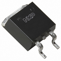
BUK135-50L,118 NXP Semiconductors, BUK135-50L,118 Datasheet - Page 2

BUK135-50L,118
Manufacturer Part Number
BUK135-50L,118
Description
TOPFET LOGIC LVL 50V D2PAK
Manufacturer
NXP Semiconductors
Series
TOPFET™r
Type
Low Sider
Datasheet
1.BUK135-50L118.pdf
(13 pages)
Specifications of BUK135-50L,118
Input Type
Non-Inverting
Number Of Outputs
1
On-state Resistance
21 mOhm
Current - Output / Channel
30A
Current - Peak Output
44A
Mounting Type
Surface Mount
Package / Case
D²Pak, TO-263 (4 leads + tab)
Lead Free Status / RoHS Status
Lead free / RoHS Compliant
Voltage - Supply
-
Operating Temperature
-
Other names
934056337118
BUK135-50L /T3
BUK135-50L /T3
BUK135-50L /T3
BUK135-50L /T3
Philips Semiconductors
LIMITING VALUES
Limiting values in accordance with the Absolute Maximum Rating System (IEC 134)
ESD LIMITING VALUE
OVERLOAD PROTECTION LIMITING VALUE
With an adequate protection supply
connected, TOPFET can protect
itself from two types of overload -
overtemperature and short circuit
load.
OVERVOLTAGE CLAMPING LIMITING VALUES
At a drain source voltage above 50 V the power MOSFET is actively turned on to clamp overvoltage transients.
1 Prior to the onset of overvoltage clamping. For voltages above this value, safe operation is limited by the overvoltage clamping energy.
2 A higher T
3 All control logic and protection functions are disabled during conduction of the source drain diode. If the protection circuit was previously
July 2002
Logic level TOPFET
SMD version of BUK124-50L
SYMBOL PARAMETER
V
I
I
I
I
P
T
T
T
SYMBOL PARAMETER
V
SYMBOL PARAMETER
V
SYMBOL PARAMETER
E
E
D
I
F
P
stg
j
sold
DS
tot
C
DS
DSM
DRM
latched, it would be reset by this condition.
j
is allowed as an overload condition but at the threshold T
Continuous voltage
Drain source voltage
Continuous currents
Drain current
Input current
Flag current
Protection supply current
Thermal
Total power dissipation
Storage temperature
Junction temperature
Mounting base temperature
Electrostatic discharge capacitor
voltage
Overload protection
Drain source voltage
Inductive load turn off
Non-repetitive clamping energy
Repetitive clamping energy
1
2
3
For overload conditions an n-MOS
transistor turns on between the
input and source to quickly
discharge the power MOSFET
gate capacitance.
CONDITIONS
V
V
V
T
continuous
during soldering
CONDITIONS
Human body model;
C = 250 pF; R = 1.5 k
REQUIRED CONDITION
protection supply
V
CONDITIONS
I
T
T
DM
mb
mb
mb
IS
PS
PS
PS
j(TO)
= 20 A; V
= 0 V
= 5 V; T
= 0 V; T
= 25˚C
= 25˚C
2
4 V
95˚C; f = 250 Hz
the over temperature trip operates to protect the switch.
mb
mb
DD
= 25˚C
= 85˚C
20 V
The drain current is limited to
reduce dissipation in case of short
circuit load. Refer to OVERLOAD
CHARACTERISTICS.
MIN.
MIN.
MIN.
MIN.
-55
-5
-5
-5
0
-
-
-
-
-
-
-
-
-
Product Specification
limited
MAX.
MAX.
MAX.
MAX.
self -
BUK135-50L
175
150
260
350
50
30
90
35
45
5
5
5
2
Rev 1.100
UNIT
UNIT
UNIT
UNIT
mA
mA
mA
mJ
mJ
kV
˚C
˚C
˚C
W
V
A
A
V


