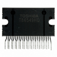
TB6549HQ Toshiba, TB6549HQ Datasheet

TB6549HQ
Specifications of TB6549HQ
Available stocks
Related parts for TB6549HQ
TB6549HQ Summary of contents
Page 1
... Built-in thermal shutdown circuit • Package: HSOP20/DIP16/HZIP25 The TB6549HQ is a Sn-plated product. (The Pb-containing materials with a high melting point that are exempted from RoHS directives are used inside the IC.) About solderability, the following conditions were confirmed (1)Use of Sn-37Pb solder Bath · ...
Page 2
Pin Assignment HSOP20-P-450-1.00 NC CcpA CcpB CcpC NC S-GND (Fin) NC IN1 IN2 NC OUT1 HZIP25-P-1.00F ...
Page 3
Block Diagram Some functional blocks, circuits or constants may be omitted or simplified in this block diagram for explanatory purposes. V reg 5 V Control logic OSC Overcurrent detecting circuit T SD Charge pump circuit CcpA CcpB Pin Functions Pin ...
Page 4
Absolute Maximum Ratings Characteristic Supply voltage Output current Input voltage FG Power dissipation PG HQ Operating temperature Storage temperature Note1: The absolute maximum ratings must be observed strictly. Make sure that no characteristic listed above ever exceeds the absolute maximum ...
Page 5
Electrical Characteristics Characteristic Supply current Input voltage Hysteresis Control circuit voltage Input current Input voltage Hysteresis voltage PWM input circuit Input current PWM frequency Minimum clock pulse width Input voltage Hysteresis Standby circuit voltage Input current Output ON-resistance Output leakage ...
Page 6
Component Description 1. Control Input/PWM Input Circuit IN1 (IN2, PWM) • The input signals are shown below. Input at the CMOS and TTL levels can be provided. Note that the input signals have a hysteresis of 0.2 V (typ.). V ...
Page 7
V CC OUT1 M GND PWM ON t1 OUT1 M PWM OFF → 300 ns (typ.) Output voltage waveform (OUT1) Note: Be sure to set the pin PWM to High when the PWM control function is not ...
Page 8
Internal Constant-Voltage (5 V) Circuit • This IC includes power supply for control circuit. • A capacitor for prevention of oscillation should be connected to S-GND associated with the pin V No other loads should be ...
Page 9
Output Circuit • This IC uses Nch MOS transistors as the upper and lower transistors in the output circuit. • As output Ω (sum for the upper and lower parts/typ.), this device of ...
Page 10
... CC (opr.) • This IC has a power monitoring function for preventing an output malfunction on power-up. However, Toshiba recommends that IN1, IN2, and SB be set to the Low level at power-on. 7. GND Sections • This IC includes two separate GND sections: S-GND for controlling and P-GND for outputting. Be sure to short-circuit these two GNDs as close to TB6549 as possible ...
Page 11
Test Circuit CC1 CC2 CC3 CC4 INH CcpA CcpB 5V PWM 5V/0V A IN1 TB6549FG/PG/ 5V/0V A IN2 I IN 5V/ INS • ...
Page 12
PWMH PWML PWMH PWML CcpA CcpB 5V/0V A PWM I 2V/0.8V PWM 100kHz IN1 5V TB6549FG/PG/HQ 0V IN2 5V SB S-GND • : PWM = 2 V/0.8 V, 100 kHz; duty: 50 ...
Page 13
(U) L (L) CcpA CcpB 5V PWM 0V IN1 TB6549FG/PG/HQ TB6549FG/PG 0V IN2 5V SB S-GND (U) F (L) CcpA CcpB 5V PWM 0V IN1 TB6549FG/PG/HQ TB6549FG/PG 0V IN2 5V ...
Page 14
ONG V CcpA CcpB 5V PWM 0V IN1 TB6549FG/PG/HQ 0V IN2 0V → • → Measure the time taken to boost the CcpA voltage up to about 29 ...
Page 15
... PCB mounting with 2.4 50% copper area) (2) IC only 1.8 (2) 1.2 0 120 Ambient temperature T P – T (TB6549HQ) ① Infinite heat sink Rθj-c = 1°C/W HEAT SINK (RθHS = 3.5°C/W) ② Rθj-c + RθHS = 4.5°C/W 60 ③ IC only Rθj-a = 39°C/W ① 40 ② ...
Page 16
... TB6549 IN2 8/7/11 SB 17/14/23 S-GND FIN/4,5,12,13,6, 20 Note 6 Note 3 TB6549FG: Pins 13, 15, 16, and 19 are not connected. TB6549HQ: Pins 13, 17, 18, 20, 21, and 22 are not connected. to S-GND. 3 and C as close to the TB6549 as possible, and the capacitor and GND lines since the IC may be destroyed TB6549FG/PG/HQ ...
Page 17
Package Dimensions Weight: 0.79 g (typ.) TB6549FG/PG/HQ 17 2010-07-13 ...
Page 18
Package Dimensions Weight: 1.11 g (typ.) TB6549FG/PG/HQ 18 2010-07-13 ...
Page 19
Package Dimensions HZIP25-1.00F Weight: 7.7 g (typ.) TB6549FG/PG/HQ 19 Unit: mm 2010-07-13 ...
Page 20
... Application Circuits The application circuits shown in this document are provided for reference purposes only. Thorough evaluation is required, especially at the mass production design stage. Toshiba does not grant any license to any industrial property rights by providing these examples of application circuits. 5. Test Circuits Components in the test circuits are used only to obtain and confirm the device characteristics. These components and circuits are not guaranteed to prevent malfunction or failure from occurring in the application equipment ...
Page 21
Points to remember on handling of ICs (1) Over current Protection Circuit Over current protection circuits (referred to as current limiter circuits) do not necessarily protect ICs under all circumstances. If the Over current protection circuits operate against the over ...
Page 22
... Product shall not be used for or incorporated into any products or systems whose manufacture, use, or sale is prohibited under any applicable laws or regulations. • The information contained herein is presented only as guidance for Product use. No responsibility is assumed by TOSHIBA for any infringement of patents or any other intellectual property rights of third parties that may result from the use of Product. No license to any intellectual property right is granted by this document, whether express or implied, by estoppel or otherwise. • ...


