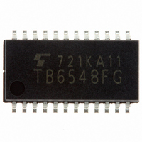
TB6548FG Toshiba, TB6548FG Datasheet

TB6548FG
Specifications of TB6548FG
Related parts for TB6548FG
TB6548FG Summary of contents
Page 1
... Forward/reverse modes • Built-in lead angle control function (0, 7.5, 15 and 30 degrees) • Built-in lap turn-on function TB6548FG: The TB6548FG is a Pb-free product. The following conditions apply to solderability: *Solderability 1. Use of Sn-37Pb solder bath *solder bath temperature = 230ºC *dipping time = 5 seconds ...
Page 2
Block Diagram PWM 3 PWM Control SEL_LAP 8 Rotation CW_CCW 4 Instruction Circuit LA0 1 Lead Angle Setting Circuit LA1 2 Clock Generator Circuit Pin Assignment CW_CCW SEL_LAP V FG_OUT Turn-on Signal Forming Circuit ...
Page 3
Pin Description Pin No. Symbol I/O Lead angle setting signal input pin • 1 LA0 I • • • 2 LA1 I • PWM signal input pin • • 3 PWM I • Rotational direction signal input pin • 4 ...
Page 4
Pin No. Symbol I/O W-phase upper turn-on signal output pin • 21 OUT_WP O • W-phase lower turn-on signal output pin • 22 OUT_WN O • Overcurrent signal input pin • • Positional signal input pin • ...
Page 5
PWM Control Upper turn-on signal (OUT-P) Lower turn-on signal (OUT-N) Output voltage of the TA84005F/FG 5 TB6548F/FG 2006-03-02 ...
Page 6
Positional Variation Since positional detection is performed in synchronization with the PWM signal, positional variation occurs in connection with the frequency of the PWM signal. Take particular care if using the IC for high-speed motors. Variation is calculated by ...
Page 7
Lead Angle Control The lead angle is 0 degrees during the starting forcible commutation and, when normal commutation is started, automatically changes to the lead angle that has been set using LA0 and LA1. However, if both LA0 and ...
Page 8
Start/Stop Control Start/Stop is controlled using the PWM signal input pin. A stop is acknowledged when the PWM signal duty is 0, and a start is acknowledged when the ON-signal of a frequency four times higher than the resonator ...
Page 9
Absolute Maximum Ratings Characteristic Power supply voltage Input voltage Turn-on signal output current Power dissipation Operating temperature Storage temperature Recommended Operating Conditions Characteristic Symbol Power supply voltage V DD Input voltage V in PWM frequency f PWM Oscillation frequency f ...
Page 10
V Electrical Characteristics Characteristic Symbol Static power supply current I DD Dynamic power supply current I DD (opr) I (H) IN-1 I (L) IN-1 Input current I (H) IN-2 I (L) IN-2 V (H) IN Input voltage ...
Page 11
Application Circuit Example = WAVE PWM signal PWM OUT_UP OUT_UN OUT_VP FG signal FG_OUT OUT_VN OUT_WP OUT_WN OC GND <TB6548F/FG> Note 1: Utmost care is necessary in the design of the output, V short-circuiting ...
Page 12
Package Dimensions Weight: 0.32 g (typ.) 12 TB6548F/FG 2006-03-02 ...
Page 13
... Application Circuits The application circuits shown in this document are provided for reference purposes only. Thorough evaluation is required, especially at the mass production design stage. Toshiba does not grant any license to any industrial property rights by providing these examples of application circuits. 5. Test Circuits Components in the test circuits are used only to obtain and confirm the device characteristics. These components and circuits are not guaranteed to prevent malfunction or failure from occurring in the application equipment ...
Page 14
TB6548F/FG 2006-03-02 ...


