LP3913SQ-AR/NOPB National Semiconductor, LP3913SQ-AR/NOPB Datasheet
LP3913SQ-AR/NOPB
Specifications of LP3913SQ-AR/NOPB


Related parts for LP3913SQ-AR/NOPB


LP3913SQ-AR/NOPB Summary of contents
Page 1
... LP3913 is available in 6x6x0 LLP package and operates over an ambient temperature range of –40°C to +85°C. © 2008 National Semiconductor Corporation Features ■ 2 low-dropout regulators -- LDO1 is used for general purpose applications, LDO2 is used for low-noise analog applications. Both LDOs have programmable output voltages. ■ ...
Page 2
Typical Application Circuit www.national.com FIGURE 1. Application Diagram 2 30000101 ...
Page 3
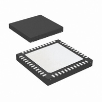
... Order Number Package Type LP3913SQ-AA 48-lead LLP LP3913SQX-AA 48-lead LLP Device Default Options Order Number LDO1 LP3913SQ-AA 2.0V LP3913SQX-AA 2.0V Device Connection Diagram 48 LLP Package (Top View) SQF48A See marking_conventions.html for more information on marking information. NSC Package Drawing Top Mark SQF48A ...
Page 4
Pin Descriptions Name I/O Type VBATT1 O A AGND G G VREFH O A LDO2EN I D VLDO2 O A VIN1 I PWR VLDO1 O A POWERACK I D ISENSE I A ADC2 I A ADC1 I ...
Page 5
Name I/O Type VDD3 I PWR VDD2 I PWR VBATT3 O A VBATT2 O A USBPWR I PWR VDD1 I PWR CHG_DET I A IREF I A Functional Description Power input to supply application. This pin must be externally shorted ...
Page 6
... Absolute Maximum Ratings If Military/Aerospace specified devices are required, please contact the National Semiconductor Sales Office/ Distributors for availability and specifications. Supply voltage range CHG_DET Voltage range USBPWR, VIN1,VIN2,VIN3,VIN4, VDD1,VDD2,VDD3 Battery voltage range VBATT1 All other pins Storage Temperature Range Power Dissipation (T = 70° ...
Page 7
Symbol Parameter t Set-Up Time for STOP Condition SU t Maximum Pulse Width of Spikes That Must Be Suppressed TRANS by the Input Filter of Both Data and CLK Signals. Li-Ion Battery Charger Electrical Characteristics Unless otherwise noted, VDD = ...
Page 8
Symbol Parameter I End-of-Charge Current EOC V Battery Restart Charging Voltage RESTARTl T Deglitch Adapter Insertion CHG_IN T Deglitch USB Power Insertion USB T Deglitch Time for Pre-qualification to Full- PQ_FULL rate Charge Transition T Deglitch Time for Full-rate to ...
Page 9
Outputs Electrical Characteristics: NRST, IRQB, ONSTAT Unless otherwise noted, VDD = 5V, VBATT = 3.6V. C normal type apply for T = 25°C. Limits appearing in boldface type apply over the entire junction temperature range for operation ...
Page 10
LDO2: Low Drop Out Linear Regulator Unless otherwise noted VIN1 = 3.6V, I 500 mΩ 100 nF. Typical values and limits appearing in normal type apply for T VREFH type apply over the entire junction temperature range for ...
Page 11
Symbol Parameter ΔV Static Output Voltage Tolerance OUT Line Regulation Load Regulation I Continuous Output Current OUT Peak Output Current Limit I Max I , PFM Mode PFM LOAD I Quiescent Current Q F Internal Oscillator Frequency OSC η Peak ...
Page 12
Symbol Parameter V ISENSE Max Voltage Scalar Output ISENSE ISENSE Min Voltage Scalar Output RANGE 0 V ISENSE Max Voltage Scalar Output ISENSE ISENSE Min Voltage Scalar Output RANGE 1 ADC1 & ADC1 & ADC2 Min Voltage Scalar Output V ...
Page 13
Typical Performance Characteristics — Battery Charger Vterm 4.2V vs. Temperature TS Pin Current vs. CHG_DET ICHG vs. VBATT CHG_DET = 5.0V, Prequal I = 500mA PROG TS Pin Current vs. Temperature 30000196 ICHG vs. VBATT CHG_DET = 5.0V, CC 30000198 ...
Page 14
ICHG vs. CHG_DET VBATT = 3.5V, CC ICHG vs. Temperature CHG_DET = 5V, VBATT = 2.5V, Prequal USB ILIMIT vs. Temperature www.national.com ICHG vs. Temperature CHG_DET = 5V, VBATT = 3.75V, CC 30000141 Thermal Regulation of Charge Current 30000143 30000145 ...
Page 15
Wall Adapter Insertion with USBPWR present CH1 = Charge Current (mA); CH3 = CHG_DET (V); CH4 = USBPWR (V) Wall Adapter Removal with USBPWR present CH1 = Charge Current (mA); CH3 = CHG_DET (V); 300001a0 15 CH4 = USBPWR (V) ...
Page 16
Typical Performance Characteristics — LDO Output Voltage Change vs Temperature (LDO1) Vin = 4.3V, Vout = 3.3V, 100 mA load Load Transient (LDO1) 3.6 Vin, 3.3 Vout, 0 – 100 mA load Line Transient (LDO1) 3.6 - 4.5 Vin, 3.3 ...
Page 17
Enable Start-up time (LDO1) 0-3.6 Vin, 3.3 Vout, 1mA load 30000152 Enable Start-up time (LDO2) 0 – 3.6 Vin, 1.8 Vout load 17 30000153 www.national.com ...
Page 18
Typical Performance Characteristics - Buck Output Voltage vs. Supply Voltage (Vout = 3.3 V) Output Voltage vs. Supply Voltage (Vout = 1.2V) Buck 1 Efficiency vs Output Current (Forced PWM Mode, Vout =1.2V, L= 2.2µH) www.national.com T = 25°C unless ...
Page 19
Buck 1 Efficiency vs Output Current (PFM to PWM mode, Vout =1.2V, L= 2.2µH) Buck 2 Efficiency vs Output Current (Forced PWM Mode, Vout =1.8V, L= 2.2µH) Buck 2 Efficiency vs Output Current (PFM to PWM Mode, Vout =1.8V, L= ...
Page 20
Buck 1 Load Transient Response VIN = 4.2V, VOUT = 1.2V ILOAD = 200-400mA (PWM Mode) Buck 2 Load Transient Response VIN = 4.2V, VOUT = 3.3V ILOAD = 200-400mA (PWM Mode) Line Transient Response Vin = 3 – 3.6 ...
Page 21
Start up into PWM Mode Vout = 1 load 30000172 Start up into PFM Mode Vout = 1 load 30000174 Start up into PWM Mode Vout = 3 load Start up ...
Page 22
Typical Performance Characteristics - Buck3 Efficiency vs. VIN ILOAD = 100mA AutoMode Efficiency vs. ILOAD VOUT = 3.3V Buck3 Load Transient Response VIN = 4.2V, VOUT = 3.3V, ILOAD = 0-100mA (PFM Mode) www.national.com T = 25°C unless otherwise noted ...
Page 23
Line Transient Response VIN = 3.6 - 4.2V, VOUT = 3.3V, ILOAD = 80mA 30000186 Line Transient Response VIN = 3.6 - 4.2V VOUT = 3.3V, ILOAD = 260mA 23 30000187 www.national.com ...
Page 24
Functional Description OPERATING MODES The LP3913 can different operating modes as illus- trated in the following Operating Mode State Diagram: State Machine Definitions V Battery low alarm threshold BLA V Battery voltage BATT WA Wall Adapter www.national.com ...
Page 25
Power Off LDO1,2 Off BUCK1,2 Off BUCK3 Off CHARGER Off A/D Converter Off NRST Low interface Off Internal System Oscillator Off Battery Monitor Off Current consumption <1 µA Power-On-Reset The LP3913 is equipped with an internal Power-On-Reset ...
Page 26
BATTLOW Register (04)h Battery Low Alarm Register D7–5 Access Read Only 0 Data reserved Reset n/a PowerOff Mode In Power Off mode the main battery, the battery charger sup- ply, and the USB supply are below their minimum on levels. ...
Page 27
Power On Timing Each timeout T1 thru to T5 are factory programmed from ms. The following defaults are shown below. Symbol Description T1 Programmable Delay for LDO1 and LDO2 T2 Programmable Delay to Buck1 T3 Programmable ...
Page 28
PON Register (00)h Power On Event Register D7–5 D4 Access Read Only 0 rw Data Reserved PACK 0: Disable Power standby, and wait for power on event. 1: Acknowledge Power On request Reset n/a 0 External Power and ...
Page 29
Transitioning From Active Mode To Standby Mode External Event Triggers the Transition from Active to Standby Mode When the device is active, a subsequent re-assertion of the push button will turn off the LP3913 indirectly by first flagging the system ...
Page 30
Transition from Active to Standby Mode Due to Expiring POWERACK Deadline With no external charger present when the system processor fails to acknowledge the power-on in time by setting either the PACK bit (D4) in the PON register or the ...
Page 31
Power Down Caused by Expiring PowerACK Deadline Transition from Charger Standby Mode to Either Active or Standby Mode While in Charger Standby mode, the battery is charged using the default values EOC, V PROG TERM and USB ...
Page 32
Compatible Serial Interface Signals The LP3913 features compatible serial interface, using two dedicated pins C_SCL and I 2 data respectively. Both signals need a pull-up resistor ac- cording ...
Page 33
C_SDA = “0” read (I 2 C_SDA = “1”) ack = acknowledge (I 2 C_SDA pulled down by either master or slave repeated start id = LP3913 chip address : 60’h ...
Page 34
LI-ION LINEAR CHARGER Charger Architecture The LP3913 can safely charge and maintain a single cell Li- Ion/Polymer battery operating off a regulated 6V Car adapter, The charger module is a linear charger with constant current pre-qualification, constant current (“CC”) full-rate ...
Page 35
Charge Status Indication Two LEDs connected to the LP3913 are used to indicate the status of the charging. The CHG pin is connected to a red LED that is enabled when an external power source is connected and the battery ...
Page 36
Full-Rate Charging Mode The full-rate charge cycle is initiated following the successful completion of the pre-qualification mode. During Full-Rate charging, the battery voltage steadily increases while charged with a constant current (CC). The three charger status bits STAT2, STAT1 and ...
Page 37
Safety Timer In order to prevent endless charging, which could degrade the battery quality and life time, the LP3913 contains a safety timer that limits charging regardless whether the battery has reached its full capacity or not. In prequalification the ...
Page 38
The current provided by the external adapter power or USB power, when inserted, first supplies the system load; the re- mainder is used for charging. The different paths are configured through two internal power FETs, Q1 and Q2, and an ...
Page 39
ANALOG TO DIGITAL CONVERTER LP3913 is equipped with an 8-bit dual-slope integrating ana- log to digital converter. Dual-slope converters provide effec- tive filtering of >500 kHz and <125 kHz noise components on the input voltage, and does not require a ...
Page 40
The source selection and the access to the conversion results are established through the linked control registers: AD- CC and ADCD as described below: ADCC Register (0a)h A/D Converter Control Register D7 D6 Access r/w r/w Data ...
Page 41
Interrupt Request Output The LP3913 has the ability to interrupt the system processor through the open drain IRQB pin, which transitions to an ac- tive logic low level upon the following 8 events: • USB Power detected • USB disconnected ...
Page 42
INTERRUPTS AND STANDBY MODE Interrupts are captured in standby mode and can be serviced when the system processor is enabled when the LP3913 active state. INTERRUPT SOURCES CHG_IN Power Detected and CHG_IN Disconnect (INT0 and INT1) An ...
Page 43
SUPPLY SPECIFICATION Supply Load LDO1 various LDO2 analog BUCK1 CPU, DSP BUCK2 IO, Logic, Memories BUCK3 Flash LINEAR LOW DROP-OUT REGULATORS (LDOS) LDO1 is a regulator that can respond to fast transients and is slated for digital loads and high ...
Page 44
LDO1 CONTROL REGISTER LDO1 can be configured through its own I The output voltage is programmable in steps of 100 mV from 1.2V to 3.3V. LDO1 gets enabled during the power-on se- quence. Disable/enable control is provided through bit D5 ...
Page 45
LDO2 CONTROL REGISTER LDO2 can be configured through its own I The output voltage is programmable in steps of 100mV from 1.3V to 3.3V. LDO2 is by default disabled and can be enabled by setting bit D5 in the control ...
Page 46
BUCK1, BUCK2: Synchronous Step Down Magnetic DC/DC Converters FUNCTIONAL DESCRIPTION The LP3913, incorporates two high efficiency synchronous switching buck regulators, BUCK1 and BUCK2 that deliver a constant voltage from a single Li-Ion battery to the portable system processors, Memory and ...
Page 47
BUCK1, BUCK2 OPERATION BUCK1 is recommended to be used as the processor core supply and has selectable output voltages ranging from 0.8V to 2.0V (Typ.). BUCK2 is recommended for IO power, Memory power and logic power. Its ...
Page 48
BUCK1 CONTROL REGISTER (05 Access Read Only 0 R/W Data Reserved Operation 0: enable/disable determined by state of BUCK1EN pin 1: enable, override BUCK1EN state Reset n/a 0 www.national.com D5 D4–0 Force PWM mode BUCK1 Output Voltage (V) ...
Page 49
BUCK2 CONTROL REGISTER (06 Access Read Only 0 R/W Data Reserved Operation 0: disabled 1: enabled Reset n D4–0 Force PWM mode BUCK2 Output Voltage (V) 0: Automatic Modulation Mode 5’h00 1: Force PWM mode 5’h01 ...
Page 50
BUCK3: Synchronous Magnetic DC/ DC Converter The LP3913 is equipped with a synchronous Buck3 magnetic DC-DC converter to supply power to the Flash memory that has a typical 1.7V-3.3V operating voltage. This voltage is low- er than the maximum battery ...
Page 51
BUCK3 CONTROL REGISTER (07 Access Read Only 0 R/W Data Reserved Force PWM 0: Automatic modulation mode 1: Force PWM modulation Reset n D4–0 Operation BUCK3 Output Voltage (V) 0: disable 5’h00 1: enable 5’h01 5’h02 ...
Page 52
Application Notes COMPONENT SELECTION Inductors for BUCK1, BUCK2 and BUCK3 There are two main considerations when choosing an induc- tor; the inductor should not saturate and the inductor current ripple is small enough to achieve the desired output voltage ripple. ...
Page 53
Graph Showing a Typical Variation in Capacitance vs. DC Bias As shown in the graph, increasing the DC Bias condition can result in the capacitance value that falls below the minimum value given in the recommended capacitor specifications ta- ble. ...
Page 54
Because the V and V are out of phase, the RMS PP-C PP-ESR value can be used to get an approximate value of the peak- to-peak ripple: Min Capacitor Unit Value μF C 4.7 VDD μF C 4.7 CHG_DET μF ...
Page 55
... USB host with a 100 mA current limit. Factory Programmable Options The following options are programmed for the LP3913. The system designer that needs specific options is advised to contact the local National Semiconductor sales office. Factory programmable options LDO1 output voltage after power up LDO2 output voltage after power up ...
Page 56
Datasheet Revision History Revision Date 1.0 08/10/2006 www.national.com Comments Initial Release, advanced specification 56 ...
Page 57
Physical Dimensions inches (millimeters) unless otherwise noted SQF48A Package: 6x6x0.8mm 48-Pin LLP Package with 0.4mm Pitch 57 www.national.com ...
Page 58
... For more National Semiconductor product information and proven design tools, visit the following Web sites at: Products Amplifiers www.national.com/amplifiers Audio www.national.com/audio Clock Conditioners www.national.com/timing Data Converters www.national.com/adc Displays www.national.com/displays Ethernet www.national.com/ethernet Interface www.national.com/interface LVDS www.national.com/lvds Power Management www.national.com/power Switching Regulators www.national.com/switchers LDOs www ...