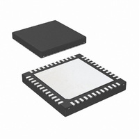
LP3913SQ-AR/NOPB National Semiconductor, LP3913SQ-AR/NOPB Datasheet - Page 4

LP3913SQ-AR/NOPB
Manufacturer Part Number
LP3913SQ-AR/NOPB
Description
IC PMU FLASH MEM PROGRMMBL 48LLP
Manufacturer
National Semiconductor
Series
PowerWise®r
Datasheet
1.LP3913SQ-ACNOPB.pdf
(58 pages)
Specifications of LP3913SQ-AR/NOPB
Applications
Handheld/Mobile Devices
Voltage - Supply
2.5 V ~ 6 V
Operating Temperature
-40°C ~ 85°C
Mounting Type
Surface Mount
Package / Case
48-LLP
Lead Free Status / RoHS Status
Lead free / RoHS Compliant
Current - Supply
-
Other names
LP3913SQ-ARTR
www.national.com
TS
VBATT1
AGND
VREFH
LDO2EN
VLDO2
VIN1
VLDO1
POWERACK
ISENSE
ADC2
ADC1
IRQB
NRST
CHG
STAT
BUCK1EN
VFB1
BCKGND1
VBUCK1
VIN2
VIN3
VBUCK2
BCKGND2
VFB2
ONOFF
I
VDDIO
I
ONSTAT
VFB3
VBUCK3
VBUCK3L2
BCK3GND1
VBUCK3L1
VIN4
USBSUSP
USBISEL
BUCK3GND2
DGND
2
2
C_SCL
C_SDA
Pin Descriptions
Name
I/O
I/O
O
G
O
O
O
O
O
O
O
G
O
O
G
O
O
G
G
G
I
I
I
I
I
I
I
I
I
I
I
I
I
I
I
I
I
I
I
I
I
Open Drain
Open Drain
Open Drain
Type
PWR
PWR
PWR
PWR
G
D
D
D
D
D
G
G
D
D
D
D
G
D
D
G
G
A
A
A
A
A
A
A
A
A
A
A
A
A
A
A
A
Battery temperature sense pin. This pin is normally connected to the thermistor
pin of the battery cell.
Positive battery terminal. This pin must be externally shorted to VBATT2 and
VBATT3
Analog Ground
Connection to bypass capacitor for internal high reference
Digital input to enable/disable LDO2
LDO2 Output
Power input to LDO1 and LDO2. VIN1 pin must be externally shorted to the VDD
pins.
LDO1 Output
Digital power acknowledgement input (see Power Sequencing)
A 4.64 kΩ resistor must be connected between this pin and GND. A fraction of
the charge current flows through this resistor to enable the A to D converter to
measure the charge current.
Channel 2 input to AD converter
Channel 1 input to AD converter
Open drain active low interrupt request
Open drain active low reset during Standby
This output indicates that a valid charger supply source (USB adapter) has been
detected, and the IC is charging. (Red LED)
Battery Status output indicator - Off during CC, 50% duty cycle during CV, 100%
duty cycle with a fully charged Li-ion battery (Green LED)
Digital input to enable/disable BUCK1
Buck1 Feedback input terminal
Buck1 Ground
Buck1 Output
Power input to BUCK1. VIN2 pin must be externally shorted to the VDD pins.
Power input to BUCK2. VIN3 pin must be externally shorted to the VDD pins.
Buck2 Output
Buck2 Ground
Buck2 Feedback input terminal
Power ON/OFF pin configured either as level (High or Low) triggered or edge
(High or Low) triggered.
I
Supply to input / output stages of digital I/O
I
Open Drain output that reflects the debounced state of ONOFF pin.
Buck3 Feedback input terminal
Buck3Output voltage
Buck3 inductor
Buck3t high current ground
Buck3 inductor
Power input to Buck3. VIN4 pin must be externally shorted to the VDD pins.
This pin needs to be pulled high during USB suspend mode.
Pulling this pin low limits the USB charge current to 100 mA. Pulling this pin high
limits the USB charge current to 500 mA.
Buck3 Core Ground
Digital ground
2
2
C compatible interface clock terminal
C compatible interface data terminal
4
Functional Description
Pin #
10
11
12
13
14
15
16
17
18
19
20
21
22
23
24
25
26
27
28
29
30
31
32
33
34
35
36
37
38
39
40
1
2
3
4
5
6
7
8
9


