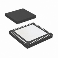
LP3913SQ-AR/NOPB National Semiconductor, LP3913SQ-AR/NOPB Datasheet - Page 45

LP3913SQ-AR/NOPB
Manufacturer Part Number
LP3913SQ-AR/NOPB
Description
IC PMU FLASH MEM PROGRMMBL 48LLP
Manufacturer
National Semiconductor
Series
PowerWise®r
Datasheet
1.LP3913SQ-ACNOPB.pdf
(58 pages)
Specifications of LP3913SQ-AR/NOPB
Applications
Handheld/Mobile Devices
Voltage - Supply
2.5 V ~ 6 V
Operating Temperature
-40°C ~ 85°C
Mounting Type
Surface Mount
Package / Case
48-LLP
Lead Free Status / RoHS Status
Lead free / RoHS Compliant
Current - Supply
-
Other names
LP3913SQ-ARTR
LDO2 CONTROL REGISTER
LDO2 can be configured through its own I
The output voltage is programmable in steps of 100mV from
1.3V to 3.3V. LDO2 is by default disabled and can be enabled
by setting bit D5 in the control register after selecting the ap-
propriate D4–0 settings, which determine the output voltage.
LDO2 can also be enabled through the external LDO2EN pin,
which is the default enable control. With a logic 0 programmed
to bit D5 in the corresponding control register, enable/disable
control is passed onto the LDO2EN pin; a logic 1 applied to
this pin enables LDO2 while a logic 0 disables the LDO2.
Setting D5 to 1 in the LDO2 control register enables LDO2,
LDO2 CONTROL REGISTER (09)h
Access
Data
Reset
D7–6
Read Only 0
Reserved
n/a
2
C control register.
D5
R/W
Operation
0: enable/ disable
determined by state of
LDO2EN pin
1: enable, override
LDO2EN state
0
45
regardless of the state of the LDO2EN pin. If the system de-
signer permanently connects the LDO2EN pin to GND, then
D5 is simply a enable/disable control bit. If the system design
permanently connects the enable pin to V
enabled during the power-on sequence and will always be on,
regardless of the state of bit D5 in the LDO2 control register.
In that particular case, the LDO2 is sequenced with the same
timing as LDO1 (see Power On sequencing).
The output voltage can be altered while LDO2 is enabled.
When LDO2 is disabled it shunts the output to A
R
SHUNT
= 200Ω (Max.).
D4–0
5’h14 –5’h1F
5’h0A
5’h0B
5’h0C
5’h0D
5’h0E
5’h00
5’h01
5’h02
5’h03
5’h04
5’h05
5’h06
5’h07
5’h08
5’h09
5’h0F
5’h10
5’h11
5’h12
5’h13
5’h14
LDO1 OutputVoltage (V)
DD
, then the LDO is
1.3
1.4
1.5
1.6
1.7
1.8
1.9
2.0
2.1
2.2
2.3
2.4
2.5
2.6
2.7
2.8
2.9
3.0
3.1
3.2
3.3
www.national.com
GND
with a


