LP3913SQ-AR/NOPB National Semiconductor, LP3913SQ-AR/NOPB Datasheet - Page 6
LP3913SQ-AR/NOPB
Manufacturer Part Number
LP3913SQ-AR/NOPB
Description
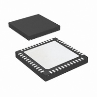
IC PMU FLASH MEM PROGRMMBL 48LLP
Manufacturer
National Semiconductor
Series
PowerWise®r
Datasheet
1.LP3913SQ-ACNOPB.pdf
(58 pages)
Specifications of LP3913SQ-AR/NOPB
Applications
Handheld/Mobile Devices
Voltage - Supply
2.5 V ~ 6 V
Operating Temperature
-40°C ~ 85°C
Mounting Type
Surface Mount
Package / Case
48-LLP
Lead Free Status / RoHS Status
Lead free / RoHS Compliant
Current - Supply
-
Other names
LP3913SQ-ARTR


www.national.com
I
V
T
T
T
VDDIO
F
V
V
V
V
F
t
t
t
t
t
t
t
Q_BATT
BF
HOLD
CLK-LP
CLK-HP
SU
DATA-HOLD
DATA-SU
SD
SDH
TH-ALERT
CLK
CLK
POR
IL
IH
OL
HYS
Absolute Maximum Ratings
If Military/Aerospace specified devices are required,
please contact the National Semiconductor Sales Office/
Distributors for availability and specifications.
Electrical Characteristics
General Electrical Characteristics
Unless otherwise noted, VDD = 5V, VBATT = 3.6V. Typical values and limits appearing in normal type apply for T
appearing in boldface type apply over the entire junction temperature range for operation, T
I
Unless otherwise noted, VDDIO = 3.6V. Typical values and limits appearing in normal type apply for T
in boldface type apply over the entire junction temperature range for operation, T
Symbol
Supply voltage range CHG_DET
Voltage range USBPWR,
Battery voltage range VBATT1, 2, 3
All other pins
Storage Temperature Range
Power Dissipation (T
ESD Rating (Note 4)
Symbol
2
C Interface Electrical Characteristics
VDD1,VDD2,VDD3
VIN1,VIN2,VIN3,VIN4,
Human Body Model:
Machine Model:
Low Level Input Voltage
High Level Input Voltage
Low Level Output Voltage
Schmitt Trigger Input Hysterisis
Clock Frequency
Bus-Free Time between START and STOP
Hold Time Repeated START Condition
CLK Low Period
CLK High Period
Set-up Time Repeated START Condition
Data Hold Time
Data Set-up Time
Battery Standby Supply Current
Power-On Reset Threshold
Thermal Shutdown Threshold
Themal Shutdown Hysteresis
Thermal Interrupt Threshold
IO Supply
Internal System Clock Frequency
A
= 70°C (Note 3)):
Parameter
Parameter
−0.3V to VDD +0.3V
−45ºC to +150ºC
−0.3V to +6.5V
−0.3V to +6.2V
−0.3V to +5V
(Notes 1, 2)
2.0 kV
2.6W
200V
All circuits off except for POR and
battery monitor. No adapter or USB
power connected.
VDD Falling Edge
6
Conditions
Operating Ratings
Thermal Information
CHG_DET
USBPWR
VBATT1, 2, 3
VIN1, VIN2, VIN3, VIN4, VDD1,
VDD2, VDD3
VDDIO
Junction Temperature (T
Ambient Temperature (T
Power Dissipation for T
Junction-to-Ambient Thermal Resistance (θ
48-pin LLP SQF48A Package (Note 7)
I
I
I
I
I
I
I
I
(Note 9)
(Note 9)
(Note 9)
(Note 9)
(Note 9)
(Note 9)
(Note 9)
2
2
2
2
2
2
2
2
C_SDA &
C_SCL
C_SDA &
C_SCL
C_SDA &
C_SCL
C_SDA &
C_SCL
Conditions
J
= 0°C to +125°C. (Notes 2, 7, 8, 9)
JjMAX
0.7VDDI
0.1VDDI
J
A
J
Min
) Range
Min
) Range
= 0°C to +125°C. (Notes 2, 7, 8, 9)
2.5
100
1.3
0.6
1.3
0.6
0.6
O
O
0
0
and T
(Notes 6, 7, 10)
J
AMAX
= 25°C. Limits appearing
Typ
160
115
Typ
1.9
20
6
2
−40°C to +125°C
−40°C to +85°C
JA
0.3VDDI
0.2VDDI
J
),
4.35V to 6.0V
= 25°C. Limits
Max
V
Max
400
2.5V to VDD
4.5V to 6.0V
2.5V to 6.0V
20
O
O
DD
0V to 4.5V
25°C/W
1.6W
Units
Units
MHz
kHz
µA
°C
°C
°C
µs
µs
µs
µs
µs
µs
ns
V
V
V
V
V
V
Related parts for LP3913SQ-AR/NOPB
Image
Part Number
Description
Manufacturer
Datasheet
Request
R

Part Number:
Description:
IC PWR MANAGEMENT W/CHRGR 48-LLP
Manufacturer:
National Semiconductor
Datasheet:
Part Number:
Description:
IC PWR MANAGEMENT W/CHRGR 48-LLP
Manufacturer:
National Semiconductor
Datasheet:
Part Number:
Description:
IC POWER MANAGEMENT 48-LLP
Manufacturer:
National Semiconductor
Datasheet:
Part Number:
Description:
IC PWR MANAGEMENT W/CHRGR 48-LLP
Manufacturer:
National Semiconductor
Datasheet:
Part Number:
Description:
IC PWR MANAGEMENT W/CHRGR 48-LLP
Manufacturer:
National Semiconductor
Datasheet:
Part Number:
Description:
IC POWER MANAGEMENT 48-LLP
Manufacturer:
National Semiconductor
Datasheet:

Part Number:
Description:
National Semiconductor [8-Bit D/A Converter]
Manufacturer:
National Semiconductor
Datasheet:
Part Number:
Description:
National Semiconductor [Media Coprocessor]
Manufacturer:
National Semiconductor
Datasheet:
Part Number:
Description:
Digitally Controlled Tone and Volume Circuit with Stereo Audio Power Amplifier, Microphone Preamp Stage and National 3D Sound
Manufacturer:
National Semiconductor
Datasheet:
Part Number:
Description:
Digitally Controlled Tone and Volume Circuit with Stereo Audio Power Amplifier, Microphone Preamp Stage and National 3D Sound
Manufacturer:
National Semiconductor
Datasheet:
Part Number:
Description:
AC97 Rev 2 Codec with Sample Rate Conversion and National 3D Sound
Manufacturer:
National Semiconductor
Part Number:
Description:
Manufacturer:
National Semiconductor
Datasheet:
Part Number:
Description:
Manufacturer:
National Semiconductor
Datasheet:
Part Number:
Description:
General Purpose, Low Voltage, Low Power, Rail-to-Rail Output Operational Amplifiers
Manufacturer:
National Semiconductor
Datasheet: