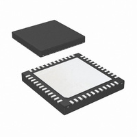
LP3913SQ-AR/NOPB National Semiconductor, LP3913SQ-AR/NOPB Datasheet - Page 33

LP3913SQ-AR/NOPB
Manufacturer Part Number
LP3913SQ-AR/NOPB
Description
IC PMU FLASH MEM PROGRMMBL 48LLP
Manufacturer
National Semiconductor
Series
PowerWise®r
Datasheet
1.LP3913SQ-ACNOPB.pdf
(58 pages)
Specifications of LP3913SQ-AR/NOPB
Applications
Handheld/Mobile Devices
Voltage - Supply
2.5 V ~ 6 V
Operating Temperature
-40°C ~ 85°C
Mounting Type
Surface Mount
Package / Case
48-LLP
Lead Free Status / RoHS Status
Lead free / RoHS Compliant
Current - Supply
-
Other names
LP3913SQ-ARTR
w = write (I
r = read (I
ack = acknowledge (I
rs = repeated start
id = LP3913 chip address : 60’h
Register Read Cycle
When a READ function is to be accomplished, a WRITE func-
tion must precede the READ function, as shown in the Read
Cycle waveform.
Multi-byte I
The LP3913’s I
ister Multi-byte command sequencing: During a multi-byte
write the Master sends the Start command followed by the
Device address, which is sent only once, followed by the 8-
bit register address, then 8 bits of data, The I
then accept the next random register address followed by 8
bits of data and continue this process until the master sends
a valid stop condition.
2
C_SDA = “1”)
2
C_SDA = “0”)
2
C Command sequence
2
C serial interface shall support Random reg-
2
C_SDA pulled down by either master or slave)
2
C slave must
I
I
2
2
C Write Cycle
C Read Cycle
33
A Typical Multi-byte random register transfer is outlined be-
low:
Device Address,
Ack Register M Address, Ack, Register M Data, Ack Reg-
ister X Address, Ack, Register X Data, Ack Register Z Ad-
dress, Ack, Register Z Data, Ack, Stop
Note: the PMIC is not required to see the I
transaction. A, M, X, and Z are random numbers
Register A Address, Ack, Register A Data,
2
C device address for each
30000112
www.national.com
30000114
30000113


