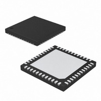
MAX8662ETM+ Maxim Integrated Products, MAX8662ETM+ Datasheet - Page 18

MAX8662ETM+
Manufacturer Part Number
MAX8662ETM+
Description
IC POWER MANAGE 48-TQFN-EP
Manufacturer
Maxim Integrated Products
Datasheet
1.MAX8662ETM.pdf
(34 pages)
Specifications of MAX8662ETM+
Applications
Handheld/Mobile Devices
Current - Supply
900µA
Voltage - Supply
4.1 V ~ 8 V
Operating Temperature
-40°C ~ 85°C
Mounting Type
Surface Mount
Package / Case
48-TQFN Exposed Pad
Lead Free Status / RoHS Status
Lead free / RoHS Compliant
Power-Management ICs for
Single-Cell, Li+ Battery-Operated Devices
18
MAX8662
______________________________________________________________________________________
4, 5
6, 7
8, 9
10
11
12
13
14
15
16
17
18
1
2
3
PIN
MAX8663
3, 4
5, 6
7, 8
—
—
10
11
12
13
—
14
15
1
2
9
NAME
SYS1,
BAT1,
OUT4
PEN1
PEN2
SYS2
BAT2
DC1,
CHG
GND
CEN
THM
ISET
EN3
DC2
BRT
REF
CT
Inp ut Li m i ter - C ontr ol Inp ut 1. U sed w i th CE N and P E N 2 to set the D C cur r ent l i m i t to 95m A,
475m A, a r esi stor p r og r am m ab l e l evel up to 2A, or to tur n off the i np ut l i m i ter ( see Tab l e 1) .
Inp ut Li m i ter - C ontr ol Inp ut 2. U sed w i th CE N and P E N 1 to set the D C cur r ent l i m i t to 95m A,
475m A, a r esi stor p r og r am m ab l e l evel up to 2A, or to tur n off the i np ut l i m i ter ( see Tab l e 1) .
Enable Input and PWM Dimming Input for Regulator 3 White LED Boost. Drive high to
enable. Drive low for more than 2ms to turn off. For PWM-controlled dimming, drive EN3
with a PWM switching input with a frequency of 1kHz to 100kHz.
DC Input Source. Connect to an AC adapter or USB source. DC1 and DC2 are internally
connected.
System Supply Voltage. The SYS output supplies power to all regulators. With no external
power, SYS1 and SYS2 connect to BAT through an internal 40mΩ switch. When a valid
voltage is present at DC_, SYS_ connects to DC_ but is limited to 5.3V. SYS1 and SYS2 are
internally connected.
Battery Connections. Connect to a single-cell Li+ battery. The battery is charged from SYS_
when a valid source is present at DC. BAT_ drives SYS_ when DC is not valid. BAT1 and
BAT2 are internally connected.
LED Analog Brightness Control Input. Connect BRT to a voltage from 50mV to 1.5V to set
I
REF and GND to set a fixed brightness when analog dimming is not required.
Charger Status Output. CHG is an open-drain nMOS that pulls low when the charger is in
fast charge or prequalification modes. CHG goes high impedance when the charger is in
top-off mode or disabled.
Charger Enable Input. Drive CEN low to enable the charger when a valid source is
connected at DC. Drive CEN high to disable charging. Drive CEN high and PEN2 low to
enter USB suspend mode.
Thermistor Input. Connect a 10kΩ negative temperature coefficient (NTC) thermistor from
THM to GND. Charging is suspended when the temperature is beyond the hot or cold
limits. Connect THM to GND to disable the thermistor functionality.
Charge Rate-Set Input. Connect a resistor from ISET to GND to set the fast-charge current
from 300mA to 1.25A. The prequalification charge current and top-off threshold are set to
10% and 7.5% of fast-charge current, respectively.
Charge Timer-Programming Pin. Connect a capacitor from CT to GND to set the length of
time required to trigger a fault condition in fast-charge or prequalification mode and to
determine the time the charger remains in top-off mode. Connect CT to GND to disable
timers.
Reference Voltage. Provides 1.5V output when EN3 is high. An internal discharge
resistance pulls REF to 0V when EN3 is low.
Ground. Low-noise ground connection.
Linear Regulator 4 Output. Delivers up to 500mA at an output voltage determined by SL1
and SL2. Connect a 4.7μF ceramic capacitor from OUT4 to GND. Increase the value to
10μF if V
CS
from 1mA to 30mA. Connect BRT to the center of a resistor-divider connected between
OUT4
< 1.5V.
FUNCTION
Pin Description


