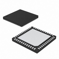
MAX8662ETM+ Maxim Integrated Products, MAX8662ETM+ Datasheet - Page 28

MAX8662ETM+
Manufacturer Part Number
MAX8662ETM+
Description
IC POWER MANAGE 48-TQFN-EP
Manufacturer
Maxim Integrated Products
Datasheet
1.MAX8662ETM.pdf
(34 pages)
Specifications of MAX8662ETM+
Applications
Handheld/Mobile Devices
Current - Supply
900µA
Voltage - Supply
4.1 V ~ 8 V
Operating Temperature
-40°C ~ 85°C
Mounting Type
Surface Mount
Package / Case
48-TQFN Exposed Pad
Lead Free Status / RoHS Status
Lead free / RoHS Compliant
Power-Management ICs for
Single-Cell, Li+ Battery-Operated Devices
skip mode, the synchronous rectifier turns off when the
inductor current falls below the n-channel zero-crossing
threshold or at the end of the switching cycle, whichev-
er occurs first.
Select an output voltage for OUT1 between 0.98V and
V
age-divider between OUT1 and GND. Choose R3
(Figure 1) for a reasonable bias current in the resistive
divider; choose R3 to be between 100kΩ and 200kΩ.
Then, R2 (Figure 1) is given by:
where V
ed using:
3.3μH and 4.7μH inductors are recommended for the
OUT1 and OUT2 step-down converters. Ensure that the
inductor saturation current rating exceeds the peak
inductor current, and the rated maximum DC inductor
current exceeds the maximum output current. For lower
load currents, the inductor current rating may be
reduced. For most applications, use an inductor with a
current rating 1.25 times the maximum required output
current. For maximum efficiency, the inductor’s DC
resistance should be as low as possible. See Table 4
for component examples.
The MAX8662 contains a boost converter, OUT3, which
drives up to seven white LEDs in series at up to 30mA.
The boost converter regulates its output voltage to
maintain the bottom of the LED stack at 320mV. A 1MHz
switching rate allows for a small inductor and small
input and output capacitors, while also minimizing input
and output ripple.
REF is a 1.5V regulated output that is available to drive
the BRT input when the boost converter is enabled.
This voltage can be used to control LED brightness by
driving BRT through a resistor-divider.
OVP limits the maximum voltage of the boost output for
protection against overvoltage due to open or discon-
nected LEDs. An external resistor between OUT3 and
OVP, with an internal 20μA pulldown current from OVP
to GND, sets the maximum boost output to:
28
IN
by connecting FB1 to the center of a resistive volt-
______________________________________________________________________________________
Boost Converter with White LED Driver
FB
V
BOOST_MAX
= 0.98V. For OUT2, R4 and R5 are calculat-
Setting OUT1 and OUT2 Output Voltage
R2 = R3 ((V
R4 = R5 ((V
Boost Overvoltage Protection (OVP)
= (R
(OUT3, MAX8662 Only)
OUT1
OUT2
OVP
OUT1 and OUT2 Inductors
x 20μA) + 1.25V
/V
/V
FB
FB
) - 1)
) - 1)
Reference Voltage
For example, with R
voltage is set at 25.25V. The OVP circuit also provides
soft-start to reduce inrush current by ramping the inter-
nal pulldown current from 0 to 20μA over 1.25ms at
startup. The 20μA internal current is disconnected
when EN3 goes low.
OUT3 can also be used as a voltage-output boost by
setting R
this, the output filter capacitor must be at least 1μF, and
the compensation network should be a 0.01μF capaci-
tor in series with a 10kΩ resistor from CC3 to ground.
LED current is set by the voltage at BRT. The V
range for adjusting output current from 1mA to 30mA is
50mV to 1.5V. Connecting BRT to a 1.5V reference volt-
age (such as REF) sets LED current to 30mA.
The EN3 input can also be driven by a logic-level PWM
brightness control signal, such as that supplied by a
microcontroller. The allowed PWM frequency range is
from 1kHz to 100kHz. A 100% duty cycle corresponds
to full current set by the BRT pin. The MAX8662 digitally
decodes the PWM brightness signal and eliminates
PWM ripple found in more common PWM brightness
controls. As a result, no external filtering is needed to
prevent intensity ripple at the PWM rate.
In order to properly distinguish between a DC or PWM
control signal, the MAX8662 delays turn-on from the ris-
ing edge of EN3, and turn-off from the falling edge of
EN3, by 2ms. If there are no more transitions in the EN3
signal after 2ms, EN3 assumes the control signal is DC
and sets LED brightness based on the DC level. If two ris-
ing edges occur within 2ms, the circuit assumes the con-
trol is PWM and sets brightness based on the duty cycle.
For the white LED driver, OUT3, a 22μH inductor is rec-
ommended for most applications. For best efficiency,
the inductor’s DC resistance should also be as low as
possible. See Table 4 for component examples.
An RC compensation network from CC3 to GND and an
output capacitor (C14 of Figure 1) ensure boost con-
verter stability. For WLED applications, connect a
0.22μF ceramic capacitor in series with a 1kΩ resistor
from CC3 to GND and use a 0.1μF output capacitor.
For fixed output voltage applications such as OLED,
connect a 0.01μF ceramic capacitor in series with a
10kΩ resistor from CC3 to GND and use a 1μF capaci-
tor. These components for fixed output voltage applica-
tions improve the load transient performance of the
boost converter. The trade-off for this improved load
OVP
for the desired output voltage. When doing
Brightness Control (Voltage or PWM)
OVP
= 1.2MΩ, the OUT3 maximum
OUT3 Compensation
OUT3 Inductor
BRT


