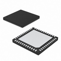
MAX8662ETM+ Maxim Integrated Products, MAX8662ETM+ Datasheet - Page 29

MAX8662ETM+
Manufacturer Part Number
MAX8662ETM+
Description
IC POWER MANAGE 48-TQFN-EP
Manufacturer
Maxim Integrated Products
Datasheet
1.MAX8662ETM.pdf
(34 pages)
Specifications of MAX8662ETM+
Applications
Handheld/Mobile Devices
Current - Supply
900µA
Voltage - Supply
4.1 V ~ 8 V
Operating Temperature
-40°C ~ 85°C
Mounting Type
Surface Mount
Package / Case
48-TQFN Exposed Pad
Lead Free Status / RoHS Status
Lead free / RoHS Compliant
transient performance is the larger (1µF) high-voltage
(30V) output capacitor.
The RC compensation network from CC3 to GND
affects the WLED driver’s sink current ramp time. As
shown in the OUT3 Enable and Disable Response
graph in the Typical Operating Characteristics section,
the OUT3 voltage ramps up in 1.25ms, but the WLED
sink current of 30mA settles in 12ms. This 12ms is
associated with the compensation of 1kΩ in series with
0.22µF. Smaller RC time constants reduce the WLED
sink current ramp time.
The MAX8662 boost converter’s high-switching fre-
quency demands a high-speed rectification diode (D1)
for optimum efficiency. A Schottky diode is recom-
mended due to its fast recovery time and low forward-
voltage drop. Ensure the diode’s peak current rating
exceeds the peak inductor current. In addition, the
diode’s reverse breakdown voltage must exceed
V
The MAX8662/MAX8663 contain four low-dropout, low-
quiescent current, low-operating voltage linear regula-
tors. The maximum output currents for OUT4, OUT5,
OUT6, and OUT7 are 500mA, 150mA, 300mA, and
150mA, respectively. Each regulator has its own enable
input. When enabled, a linear regulator soft-starts by
ramping the outputs at 34V/ms. This limits inrush cur-
rent when the regulators are enabled.
The LDO output voltages, OUT4, OUT5, OUT6, and
OUT7 are pin programmable by SL1 and SL2 (Table 3).
SL1 and SL2 are intended to be hardwired and cannot
be driven by active logic. Changes to SL1 and SL2
after power-up are ignored.
Table 3. SL1 and SL2, Output Voltage Selection
OUT3
Open circuit
Open circuit
Open circuit
. See Table 4 for component examples.
Ground
Ground
Ground
SL1
SYS
SYS
SYS
CONNECT SL_ TO:
(OUT4, OUT5, OUT6, and OUT7)
Single-Cell, Li+ Battery-Operated Devices
______________________________________________________________________________________
Open circuit
Open circuit
Open circuit
Ground
Ground
Ground
SL2
SYS
SYS
SYS
OUT3 Diode Selection
Linear Regulators
OUT4 (V)
2.85
3.3
3.3
3.3
2.5
2.5
1.2
3.3
1.8
Power-Management ICs for
LINEAR REGULATOR OUTPUT VOLTAGES
VL is the output of a 3.3V linear regulator that powers
the on-chip input limiter and charger control circuitry.
VL is powered from DC and can provide up to 10mA
when a DC source is present. Bypass VL to GND with a
0.1µF capacitor.
The OUT1–OUT7 regulators have individual enable
inputs. Drive EN_ high to initiate soft-start and enable
OUT_. Drive EN_ low to disable OUT_. When disabled,
each regulator (OUT1–OUT7) switches in an active
pulldown resistor to discharge the output.
The MAX8662/MAX8663 implement soft-start on many
levels to control inrush current and avoid collapsing
source supply voltages. The input-voltage limit and bat-
tery charger have a 1.5ms soft-start time. All regulators
also implement soft-start. White LED driver soft-start is
accomplished by ramping the OVP current from 0 to
20µA in 1.25ms. During soft-start, the PWM controller
forces 0% switching duty cycle to avoid an input cur-
rent surge at turn-on.
When the DC voltage is below the DC undervoltage
threshold (V
MAX8662/MAX8663 enter DC undervoltage lockout (DC
UVLO). DC UVLO forces the power management cir-
cuits to a known dormant state until the DC voltage is
high enough to allow the device to make accurate deci-
sions. In DC UVLO, Q1 is open (Figure 2), the charger is
disabled, POK is high-Z, and CHG is high-Z. The sys-
tem load switch, Q2 (Figure 2) is closed in DC UVLO,
allowing the battery to power the SYS node. All regula-
tors are allowed to operate from the battery in DC UVLO.
OUT5 (V)
Undervoltage and Overvoltage Lockout
2.85
2.85
2.85
2.85
3.3
3.3
3.3
1.8
2.5
UVLO_DC
Regulator Enable Inputs (EN_)
OUT6 (V)
Soft-Start/Inrush Current
, typically 3.5V falling), the
1.85
1.85
2.85
3.3
1.5
1.5
1.1
1.5
3.3
VL Linear Regulator
OUT7 (V)
1.85
1.85
1.85
2.85
3.3
1.5
1.3
1.3
1.5
DC UVLO
29


