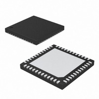
MAX8662ETM+ Maxim Integrated Products, MAX8662ETM+ Datasheet - Page 30

MAX8662ETM+
Manufacturer Part Number
MAX8662ETM+
Description
IC POWER MANAGE 48-TQFN-EP
Manufacturer
Maxim Integrated Products
Datasheet
1.MAX8662ETM.pdf
(34 pages)
Specifications of MAX8662ETM+
Applications
Handheld/Mobile Devices
Current - Supply
900µA
Voltage - Supply
4.1 V ~ 8 V
Operating Temperature
-40°C ~ 85°C
Mounting Type
Surface Mount
Package / Case
48-TQFN Exposed Pad
Lead Free Status / RoHS Status
Lead free / RoHS Compliant
Power-Management ICs for
Single-Cell, Li+ Battery-Operated Devices
When the DC voltage is above the DC overvoltage
threshold (V
MAX8663 enter DC overvoltage lockout (DC OVLO).
DC OVLO mode protects the MAX8662/MAX8663 and
downstream circuitry from high-voltage stress up to 9V.
In DC OVLO, VL is on, Q1 (Figure 2) is open, the charg-
er is disabled, POK is high-Z, and CHG is high-Z. The
system load switch Q2 (Figure 2) is closed in DC
OVLO, allowing the battery to power SYS. All regulators
are allowed to operate from the battery in DC OVLO.
When the SYS voltage falls below the SYS undervoltage
threshold (V
MAX8662/MAX8663 enter SYS undervoltage lockout
(SYS UVLO). SYS UVLO forces all regulators off. All
regulators assume the states determined by the corre-
sponding enable input (EN_) when the SYS voltage
rises above V
The MAX8662/MAX8663 reduce input-limiter current by
5%/°C when its die temperature exceeds +100°C. The
system load (SYS) has priority over charger current, so
input current is first reduced by lowering charge cur-
rent. If the junction temperature still reaches +120°C in
spite of charge-current reduction, no current is drawn
from DC, the battery supplies the entire system load,
and SYS is regulated at 100mV below BAT. Note that
this on-chip thermal-limiting circuitry is not related to,
and operates independently from, the thermistor input.
Table 4. External Components List (See Figure 1)
30
COMPONENT
C2, C3
C4, C6
C5, C7
C8, C9
______________________________________________________________________________________
C10
C11
C12
C1
OVLO_DC
UVLO_SYS
UVLO_SYS
Input filter capacitor
VL filter capacitor
Buck input bypass capacitors
Step-down output filter
capacitors
Linear regulator input filter
capacitors
SYS output bypass capacitor
Battery bypass capacitor
Charger timing capacitor
, typically 6.9V), the MAX8662/
Input-Limiter Thermal Limiting
.
FUNCTION
, typically 2.4V falling), the
SYS UVLO
4.7μF ± 10% , 16V X 5R cer am i c cap aci tor
M ur ata G RM 188R61C 105KA93B or Tai yo Y ud en E M K107 BJ105KA
0.1μF ±10%, 10V X5R ceramic capacitor (0402)
Murata GRM 155R61A104KA01 or TDK C1005X5R1A104K
4.7μF ±10%, 6.3V X5R ceramic capacitors (0603)
Mutara GRM188R60J475KE
2 x 10μF ±10%, 6.3V X5R ceramic capacitors (0805)
Murata GRM219R60J106KE19
1.0μF ± 10% , 16V X 5R cer am i c cap aci tor s ( 0603)
M ur ata G RM 188R61C 105KA93B or Tai yo Y ud en E M K107 BJ105KA
10μF ±10%, 6.3V X5R ceramic capacitor
4.7μF ±10%, 6.3V X5R ceramic capacitor
0.068μF ±10%, 10V X5R ceramic capacitor (0402)
TDK C1005X5R1A683K
DC OVLO
The MAX8662/MAX8663 disable all charger, SYS, and
regulator outputs (except VL) if the junction tempera-
ture rises above +165°C, allowing the device to cool.
When the junction temperature cools by approximately
15°C, resume the state they held prior to thermal over-
load. Note that this on-chip thermal-protection circuitry
is not related to, and operates independently from, the
thermistor input. Also note that thermal-overload shut-
down is a fail-safe mechanism. Proper thermal design
should ensure that the junction temperature of the
MAX8662/MAX8663 never exceeds the absolute maxi-
mum rating of +150°C.
The input capacitor in a DC-DC converter reduces cur-
rent peaks drawn from the battery or other input power
source and reduces switching noise in the controller.
The impedance of the input capacitor at the switching
frequency should be less than the input source’s output
impedance so that high-frequency switching currents
do not pass through the input source. The DC-DC con-
verter output capacitor keeps output ripple small and
ensures control-loop stability. The output capacitor must
also have low impedance at the switching frequency.
Ceramic capacitors with X5R or X7R dielectrics are
highly recommended for both input and output capaci-
tors due to their small size, low ESR, and small tempera-
ture coefficients.
See Table 4 for example OUT1/OUT2 input and output
capacitors and manufacturers.
Step-Down Converters (OUT1 and OUT2)
Regulator Thermal-Overload Shutdown
Applications Information
PART
Capacitor Selection


