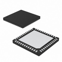
MAX8662ETM+ Maxim Integrated Products, MAX8662ETM+ Datasheet - Page 32

MAX8662ETM+
Manufacturer Part Number
MAX8662ETM+
Description
IC POWER MANAGE 48-TQFN-EP
Manufacturer
Maxim Integrated Products
Datasheet
1.MAX8662ETM.pdf
(34 pages)
Specifications of MAX8662ETM+
Applications
Handheld/Mobile Devices
Current - Supply
900µA
Voltage - Supply
4.1 V ~ 8 V
Operating Temperature
-40°C ~ 85°C
Mounting Type
Surface Mount
Package / Case
48-TQFN Exposed Pad
Lead Free Status / RoHS Status
Lead free / RoHS Compliant
Power-Management ICs for
Single-Cell, Li+ Battery-Operated Devices
The MAX8662/MAX8663 have a thermal-limiting circuitry,
as well as a shutdown feature to protect the IC from dam-
age when the die temperature rises. To allow the maxi-
mum charging current and load current on each
regulator, and to prevent thermal overload, it is important
to ensure that the heat generated by the
MAX8662/MAX8663 is dissipated into the PCB. The pack-
age’s exposed paddle must be soldered to the PCB, with
multiple vias tightly packed under the exposed paddle to
ensure optimum thermal contact to the ground plane.
Table 5 shows the thermal characteristics of the
MAX8662/MAX8663 packages. For example, the junc-
tion-to-case thermal resistance (θ
1.7°C/W. When properly mounted on a multilayer PCB,
the junction-to-ambient thermal resistance (θ
cally 28°C/W.
High switching frequencies and relatively large peak
currents make the PCB layout a very important aspect of
design. Good design minimizes ground bounce, exces-
sive EMI on the feedback paths, and voltage gradients
Table 5. MAX8662/MAX8663 Package Thermal Characteristics
32
CONTINUOUS
POWER
DISSIPATION
θ
θ
JA
JC
______________________________________________________________________________________
2105.3mW
Derate 26.3mW/°C above
+70°C
38°C/W
1.4°C/W
SINGLE-LAYER PCB
PCB Layout and Routing
48-PIN THIN QFN (6mm x 6mm)
Power Dissipation
JC
) of the MAX8663 is
2963.0mW
Derate 37.0mW/°C above
+70°C
27°C/W
1.4°C/W
MULTILAYER PCB
JA
) is typi-
in the ground plane, which can result in instability or
regulation errors.
A separate low-noise analog ground plane containing
the reference, linear regulator, signal ground, and GND
must connect to the power-ground plane at only one
point to minimize the effects of power-ground currents.
PG_, DC power, and battery grounds must connect
directly to the power-ground plane. Connect GND to
the exposed paddle directly under the IC. Use multiple
tightly spaced vias to the ground plane under the
exposed paddle to help cool the IC.
Position input capacitors from DC, SYS, BAT, PV1, and
PV2 to the power-ground plane as close as possible to
the IC. Connect input capacitors and output capacitors
from inputs of linear regulators to low-noise analog
ground as close as possible to the IC. Connect the
inductors, output capacitors, and feedback resistors as
close to the IC as possible and keep the traces short,
direct, and wide.
Refer to the MAX8662/MAX8663 evaluation kit for a
suitable PCB layout example.
1777.8mW
Derate 22.2mW/°C above
+70°C
45°C/W
1.7°C/W
SINGLE-LAYER PCB
40-PIN THIN QFN (5mm x 5mm)
2857.1mW
Derate 35.7mW/°C above
+70°C
28°C/W
1.7°C/W
MULTILAYER PCB


