L9953 STMicroelectronics, L9953 Datasheet - Page 27
L9953
Manufacturer Part Number
L9953
Description
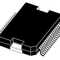
IC DVR DOOR ACTUATOR POWERSO-36
Manufacturer
STMicroelectronics
Datasheet
1.L9953XPTR.pdf
(38 pages)
Specifications of L9953
Applications
Door Actuator
Current - Supply
7mA
Voltage - Supply
7 V ~ 28 V
Operating Temperature
-40°C ~ 150°C
Mounting Type
Surface Mount
Package / Case
PowerSO-36 Exposed Bottom Pad
Mounting Style
SMD/SMT
Lead Free Status / RoHS Status
Lead free / RoHS Compliant
Available stocks
Company
Part Number
Manufacturer
Quantity
Price

Part Number:
L9953EXP
Manufacturer:
ST
Quantity:
20 000
Part Number:
L9953LXP
Manufacturer:
ST
Quantity:
20 000
Part Number:
L9953LXPTR
Manufacturer:
ST
Quantity:
20 000
Part Number:
L9953XP
Manufacturer:
ST
Quantity:
20 000
Company:
Part Number:
L9953XPTR
Manufacturer:
st
Quantity:
1 699
Part Number:
L9953XPTR
Manufacturer:
ST
Quantity:
20 000


L9953 / L9953XP
Table 19.
Bit
17
16
15
14
13
12
11
10
9
8
7
6
5
4
3
2
1
0
x (don’t care)
x (don’t care)
x (don’t care)
x (don’t care)
OUT8 – HS
OUT7 – HS
OUT6 – HS
OUT5 – HS
OUT4 – HS
OUT3 – HS
OUT2 – HS
OUT1 – HS
OUT5 – LS
OUT4 – LS
OUT3 – LS
OUT2 – LS
OUT1 – LS
Name
on/off
on/off
on/off
on/off
on/off
on/off
on/off
on/off
on/off
on/off
on/off
on/off
on/off
SPI - input data and Status registers 0 (continued)
Input register 0 (write)
If a bit is set the selected
output driver is switched
on. If the corresponding
PWM enable bit is set
(Input Register 1) the
driver is only activated if
PWM1 (PWM2) input
signal is high. The outputs
of OUT1-OUT5 are half
bridges. If the bits of HS-
and LS-driver of the same
half bridge are set, the
internal logic prevents that
both drivers of this output
stage can be switched on
simultaneously in order to
avoid a high internal
current from VS to GND.
In test mode (CSN>9.5V)
this bit combinations are
used to multiplex internal
signals to the DO-output.
LS3 HS3 LS4 HS4 LS5 HS5 CM/PWM2
0
1
0
1
0
1
0
0
1
0
1
0
1
0
0
1
1
0
1
Comment
Doc ID 14278 Rev 3
0
0
1
1
0
1
0
0
0
0
1
1
0
0
0
0
1
1
5µA Iref
Tsens1
Tsens2
Tsens3
Tsens4
Vbgp
over-current
over-current
over-current
over-current
over-current
over-current
over-current
over-current
over-current
over-current
over-current
over-current
over-current
OUT8 – HS
OUT7 – HS
OUT6 – HS
OUT5 – HS
OUT4 – HS
OUT3 – HS
OUT2 – HS
OUT1 – HS
OUT5 – LS
OUT4 – LS
OUT3 – LS
OUT2 – LS
OUT1 – LS
No error bit
Name
0
0
0
Functional description of the SPI
Status register 0 (read)
In case of an over-current
event the corresponding status
bit is set and the output driver
is disabled. If the over-current
Recovery Enable bit is set
(Input Register 1) the output
will be automatically
reactivated after a delay time
resulting in a PWM modulated
current with a programmable
duty cycle (Bit 21).
If the over-current recovery bit
is not set the microcontroller
has to clear the over-current
bit (Reset Bit) to reactivate the
output driver.
A logical NOR-combination of
all bits 1 to 22 in both status
registers.
Comment
27/38
Related parts for L9953
Image
Part Number
Description
Manufacturer
Datasheet
Request
R

Part Number:
Description:
STMicroelectronics [RIPPLE-CARRY BINARY COUNTER/DIVIDERS]
Manufacturer:
STMicroelectronics
Datasheet:
Part Number:
Description:
STMicroelectronics [LIQUID-CRYSTAL DISPLAY DRIVERS]
Manufacturer:
STMicroelectronics
Datasheet:

Part Number:
Description:
BOARD EVAL FOR MEMS SENSORS
Manufacturer:
STMicroelectronics
Datasheet:
Part Number:
Description:
NPN TRANSISTOR POWER MODULE
Manufacturer:
STMicroelectronics
Datasheet:
Part Number:
Description:
TURBOSWITCH ULTRA-FAST HIGH VOLTAGE DIODE
Manufacturer:
STMicroelectronics
Datasheet:
Part Number:
Description:
Manufacturer:
STMicroelectronics
Datasheet:
Part Number:
Description:
DIODE / SCR MODULE
Manufacturer:
STMicroelectronics
Datasheet:
Part Number:
Description:
DIODE / SCR MODULE
Manufacturer:
STMicroelectronics
Datasheet:
Part Number:
Description:
Search -----> STE16N100
Manufacturer:
STMicroelectronics
Datasheet:
Part Number:
Description:
Search ---> STE53NA50
Manufacturer:
STMicroelectronics
Datasheet:
Part Number:
Description:
NPN Transistor Power Module
Manufacturer:
STMicroelectronics
Datasheet:
Part Number:
Description:
DIODE / SCR MODULE
Manufacturer:
STMicroelectronics
Datasheet: