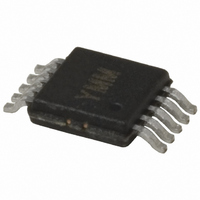
MIC2169BYMM Micrel Inc, MIC2169BYMM Datasheet - Page 11

MIC2169BYMM
Manufacturer Part Number
MIC2169BYMM
Description
IC CTLR PWM BUCK SYNC 10MSOP
Manufacturer
Micrel Inc
Datasheet
1.MIC2169BYMM.pdf
(25 pages)
Specifications of MIC2169BYMM
Pwm Type
Voltage Mode
Number Of Outputs
1
Frequency - Max
550kHz
Duty Cycle
92%
Voltage - Supply
3 V ~ 14.5 V
Buck
Yes
Boost
No
Flyback
No
Inverting
No
Doubler
No
Divider
No
Cuk
No
Isolated
No
Operating Temperature
-40°C ~ 85°C
Package / Case
10-MSOP, Micro10™, 10-uMAX, 10-uSOP
Frequency-max
550kHz
Lead Free Status / RoHS Status
Lead free / RoHS Compliant
Other names
576-3641-5
MIC2169BYMM
MIC2169BYMM
Available stocks
Company
Part Number
Manufacturer
Quantity
Price
Part Number:
MIC2169BYMM
Manufacturer:
MICREL/麦瑞
Quantity:
20 000
Application Information
MOSFET Selection
The MIC2169B controller works from input voltages of
3V to 14.5V and has an internal 5V regulator to provide
power to turn the external N-Channel power MOSFETs
for high- and low-side switches. For applications where
V
mode, and it is necessary that the power MOSFETs
used are sub-logic level and are in full conduction mode
for V
level MOSFETs, whose operation is specified at V
4.5V must be used. For the lower (<5V) applications, the
V
increase the driver voltage to the MOSFET.
It is important to note the on-resistance of a MOSFET
increases with increasing temperature. A 75°C rise in
junction temperature will increase the channel resistance
of the MOSFET by 50% to 75% of the resistance
specified at 25°C. This change in resistance must be
accounted
dissipation and in calculating the value of current-sense
(CS) resistor. Total gate charge is the charge required to
turn the MOSFET on and off under specified operating
conditions (V
the MIC2169B gate-drive circuit. At 500kHz switching
frequency and above, the gate charge can be a
significant source of power dissipation in the MIC2169B.
At low output load, this power dissipation is noticeable
as a reduction in efficiency. The average current
required to drive the high-side MOSFET is:
where:
The low-side MOSFET is turned on and off at V
because the freewheeling diode is conducting during this
time. The switching loss for the low-side MOSFET is
usually negligible. Also, the gate-drive current for the
low-side MOSFET is more accurately calculated using
CISS at V
For the low-side MOSFET:
Since the current from the gate drive comes from the
input voltage, the power dissipated in the MIC2169B due
to gate drive is:
Micrel, Inc.
April 2010
IN
DD
< 5V, the internal V
I
current.
Q
taken from manufacturer’s data sheet for V
I
I
P
G[high-side](avg)
supply can be connected directly to V
[ G
[ G
GS
GATEDRIVE
G
low
high
= total gate charge for the high-side MOSFET
of 2.5V. For applications when V
−
DS
−
side
side
= 0 instead of gate charge.
for
DS
](
](
avg
and V
avg
= average high-side MOSFET gate
=
when
)
)
V
=
=
IN
C
GS
Q
ISS
×
). The gate charge is supplied by
DD
G
(
I
calculating
[ G
×
×
regulator operates in dropout
high
f
V
S
GS
−
side
×
f
S
](
avg
MOSFET
)
+
IN
I
[ G
> 5V; logic-
low
IN
GS
−
to help
= 5V.
side
DS
power
GS
](
= 0
avg
=
)
)
11
A convenient figure of merit for switching MOSFETs is
the on resistance times the total gate charge R
Lower numbers translate into higher efficiency. Low
gate-charge logic-level MOSFETs are a good choice for
use with the MIC2169B.
Parameters that are important to MOSFET switch
selection are:
The voltage ratings for the top and bottom MOSFET are
essentially equal to the input voltage. A safety factor of
20% should be added to the V
to account for voltage spikes due to circuit parasitics.
The power dissipated in the switching transistor is the
sum of the conduction losses during the on-time
(P
the period of time when the MOSFETs turn on and off
(P
where:
Making the assumption the turn-on and turn-off transition
times
approximated by:
where:
The total high-side MOSFET switching loss is:
where:
The low-side MOSFET switching losses are negligible
and can be ignored for these calculations.
CONDUCTION
AC
).
• Voltage rating
• On-resistance
• Total gate charge
R
D = duty cycle =
C
I
P
P
P
t
G
P
t
50ns)
V
f
T
T
S
SW
CONDUCTION
AC
SW
ISS
AC
D
are
= gate-drive current (1.4A for the MIC2169B)
it the switching frequency, nominally 500kHz
= switching transition time (typically 20ns to
=
= freewheeling diode drop, typically 0.5V
= on-resistance of the MOSFET switch
and C
=
C
=
=
) and the switching losses that occur during
P
ISS
P
(
V
AC
equal;
CONDUCTION
IN
×
(
OSS
off
+
V
GS
V
)
are measured at V
=
+
D
I
I
P
)
⎛
⎜ ⎜
⎝
+
G
SW
the
×
AC
V
V
C
I
IN
PK
O
(
OSS
(
rms
on
+
⎞
⎟ ⎟
⎠
×
transition
)
P
)
t
AC
2
×
T
DS
×
V
×
IN
R
(max) of the MOSFETs
f
S
SW
DS
M9999-041210-B
times
= 0
MIC2169B
DS(ON)
can
×Q
be
G
.


