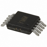
MIC2169BYMM Micrel Inc, MIC2169BYMM Datasheet - Page 17

MIC2169BYMM
Manufacturer Part Number
MIC2169BYMM
Description
IC CTLR PWM BUCK SYNC 10MSOP
Manufacturer
Micrel Inc
Datasheet
1.MIC2169BYMM.pdf
(25 pages)
Specifications of MIC2169BYMM
Pwm Type
Voltage Mode
Number Of Outputs
1
Frequency - Max
550kHz
Duty Cycle
92%
Voltage - Supply
3 V ~ 14.5 V
Buck
Yes
Boost
No
Flyback
No
Inverting
No
Doubler
No
Divider
No
Cuk
No
Isolated
No
Operating Temperature
-40°C ~ 85°C
Package / Case
10-MSOP, Micro10™, 10-uMAX, 10-uSOP
Frequency-max
550kHz
Lead Free Status / RoHS Status
Lead free / RoHS Compliant
Other names
576-3641-5
MIC2169BYMM
MIC2169BYMM
Available stocks
Company
Part Number
Manufacturer
Quantity
Price
Part Number:
MIC2169BYMM
Manufacturer:
MICREL/麦瑞
Quantity:
20 000
Figure 17 shows MIC2169B startup with a pre-bias of
2.2V on the output (90% of V
output voltage discharge.
Design and PCB Layout Guideline
WARNING!!! TO MINIMIZE EMI AND OUTPUT NOISE,
FOLLOW THESE LAYOUT RECOMMENDATIONS:
PCB Layout is critical to achieve reliable, stable and
efficient performance. A ground plane is required to
control EMI and minimize the inductance in power,
signal and return paths.
The following guidelines should be followed to insure
proper operation of the MIC2169B converter.
IC
•
•
•
Input Capacitor
•
•
Micrel, Inc.
April 2010
Figure 17. MIC2169B Startup with Pre-Bias Support,
Place the IC and MOSFETs close to the point of
load (POL).
Use fat traces to route the input and output power
lines.
Signal and power grounds should be kept separate
and connected at only one location.
Place the V
Place the V
the board and as close to the MOSFETs as
possible.
Pre-Bias At 90% of V
IN
IN
input capacitor next.
input capacitors on the same side of
OUT
) without the pre-existing
OUT_FINAL
17
•
•
•
•
•
•
•
•
Inductor
•
•
•
•
Output Capacitor
•
•
•
Keep both the V
short.
Place several vias to the ground plane close to the
V
Use either X7R or X5R dielectric input capacitors.
Do not use Y5V or Z5U type capacitors.
Do not replace the ceramic input capacitor with any
other type of capacitor. Any type of capacitor can be
placed in parallel with the input capacitor.
If a Tantalum input capacitor is placed in parallel
with the input capacitor, it must be recommended for
switching regulator applications and the operating
voltage must be derated by 50%.
In “Hot-Plug” applications, a Tantalum or Electrolytic
bypass capacitor must be used to limit the over-
voltage spike seen on the input supply with power is
suddenly applied.
An additional Tantalum or Electrolytic bypass input
capacitor of 22uF or higher is required at the input
power connection.
Use a 5Ω resistor from the input supply to the V
pin on the MIC2169B. Also, place a 1µF ceramic
capacitor from this pin to GND, preferably not
through a via. The capacitor must be located right at
the IC. The V
placement
Connections must be made with wide trace.
Keep the inductor connection to the switch node
(SW) short.
Do not route any digital lines underneath or close to
the inductor.
Keep the switch node (SW) away from the feedback
(FB) pin.
To minimize noise, place a ground plane underneath
the inductor.
Use a wide trace to connect the output capacitor
ground terminal to the input capacitor ground
terminal.
Phase margin will change as the output capacitor
value and ESR changes. Contact the factory if the
output capacitor is different from what is shown in
the BOM.
The feedback trace should be separate from the
power trace and connected as close as possible to
the output capacitor. Sensing a long high-current
load trace can degrade the DC load regulation.
IN
input capacitor ground terminal.
of
dd
terminal is very noise sensitive and
the
IN
and power GND connections
capacitor
is
M9999-041210-B
very
MIC2169B
critical.
DD


