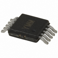
MIC2169BYMM Micrel Inc, MIC2169BYMM Datasheet - Page 13

MIC2169BYMM
Manufacturer Part Number
MIC2169BYMM
Description
IC CTLR PWM BUCK SYNC 10MSOP
Manufacturer
Micrel Inc
Datasheet
1.MIC2169BYMM.pdf
(25 pages)
Specifications of MIC2169BYMM
Pwm Type
Voltage Mode
Number Of Outputs
1
Frequency - Max
550kHz
Duty Cycle
92%
Voltage - Supply
3 V ~ 14.5 V
Buck
Yes
Boost
No
Flyback
No
Inverting
No
Doubler
No
Divider
No
Cuk
No
Isolated
No
Operating Temperature
-40°C ~ 85°C
Package / Case
10-MSOP, Micro10™, 10-uMAX, 10-uSOP
Frequency-max
550kHz
Lead Free Status / RoHS Status
Lead free / RoHS Compliant
Other names
576-3641-5
MIC2169BYMM
MIC2169BYMM
Available stocks
Company
Part Number
Manufacturer
Quantity
Price
Part Number:
MIC2169BYMM
Manufacturer:
MICREL/麦瑞
Quantity:
20 000
The voltage rating of capacitor should be twice the
voltage for a tantalum and 20% greater for aluminum
electrolytic.
The output capacitor RMS current is calculated below:
The power dissipated in the output capacitor is:
Input Capacitor Selection
The input capacitor should be selected for ripple current
rating and voltage rating. Tantalum input capacitors may
fail when subjected to high inrush currents, caused by
turning the input supply on. A tantalum input capacitor’s
voltage rating should be at least 2 times the maximum
input
electrolytic, OS-CON, and multilayer polymer film
capacitors can handle the higher inrush currents without
voltage derating. The input voltage ripple will primarily
depend on the input capacitor’s ESR. The peak input
current is equal to the peak inductor current, so:
The input capacitor must be rated for the input current
ripple. The RMS value of input capacitor current is
determined at the maximum output current. Assuming
the peak-to-peak inductor ripple current is low:
The power dissipated in the input capacitor is:
Voltage Setting Components
The MIC2169B requires two resistors to set the output
voltage as shown in Figure 6.
Micrel, Inc.
April 2010
I
P
I
P
Δ
C
C
DISS
DISS
V
OUT
IN
IN
(
voltage
rms
(
rms
Figure 6. Voltage-Divider Configuration
(
=
(
)
C
C
)
≈
I
IN
OUT
INDUCTOR
MIC2169B
=
I
)
OUT
)
=
I
PP
=
12
(
I
(max)
CIN
to
(
I
C
Error
Amp
OUT
(
rms
(
peak
maximize
×
(
rms
)
)
)
D
2
0.8V
V
)
)
2
×
REF
×
×
×
R
R
(
R
1
ESR
ESR
−
ESR
D
(
(
)
reliability.
C
(
C
C
IN
IN
OUT
)
)
FB
5
)
R1
R2
Aluminum
13
The output voltage is determined by the equation:
where
A typical value of R1 can be between 3kΩ and 10kΩ. If
R1 is too large, it may allow noise to be introduced into
the voltage feedback loop. If R1 is too small, in value, it
will decrease the efficiency of the power supply,
especially at light loads. Once R1 is selected, R2 can be
calculated using:
External Schottky Diode
An external freewheeling diode is used to keep the
inductor current flow continuous while both MOSFETs
are turned off. This dead time prevents current from
flowing unimpeded through both MOSFETs and is
typically 50ns. The diode conducts twice during each
switching cycle. Although the average current through
this diode is small, the diode must be able to handle the
peak current.
The reverse voltage requirement of the diode is:
The power dissipated by the Schottky diode is:
where:
The external Schottky diode, D1, is not necessary for
circuit operation since the low-side MOSFET contains a
parasitic body diode. The external diode will improve
efficiency and decrease high frequency noise. If the
MOSFET body diode is used, it must be rated to handle
the peak and average current. The body diode has a
relatively slow reverse recovery time and a relatively
high forward voltage drop. The power lost in the diode is
proportional to the forward voltage drop of the diode. As
the high-side MOSFET starts to turn on, the body diode
becomes a short circuit for the reverse recovery period,
dissipating additional power. The diode recovery and the
circuit inductance will cause ringing during the high-side
MOSFET turn-on. An external Schottky diode conducts
at a lower forward voltage preventing the body diode in
the MOSFET from turning on. The lower forward voltage
drop dissipates less power than the body diode. The lack
of a reverse recovery mechanism in a Schottky diode
causes less ringing and less power loss.
V
I
V
P
V
R
V
D(avg)
REF
DIODE(rrm)
DIODE
F
O
2
= forward voltage at the peak diode current
=
=
for the MIC2169B is typically 0.8V
= I
V
V
V
= I
REF
O
REF
OUT
D(avg)
−
= V
×
V
× 2 × 50ns × f
×
⎛
⎜
⎝
REF
IN
1
R
× V
+
1
R
R
F
2
1
⎞
⎟
⎠
S
M9999-041210-B
MIC2169B


