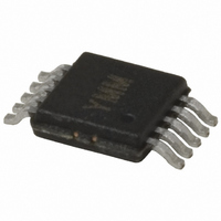
MIC2169BYMM Micrel Inc, MIC2169BYMM Datasheet - Page 9

MIC2169BYMM
Manufacturer Part Number
MIC2169BYMM
Description
IC CTLR PWM BUCK SYNC 10MSOP
Manufacturer
Micrel Inc
Datasheet
1.MIC2169BYMM.pdf
(25 pages)
Specifications of MIC2169BYMM
Pwm Type
Voltage Mode
Number Of Outputs
1
Frequency - Max
550kHz
Duty Cycle
92%
Voltage - Supply
3 V ~ 14.5 V
Buck
Yes
Boost
No
Flyback
No
Inverting
No
Doubler
No
Divider
No
Cuk
No
Isolated
No
Operating Temperature
-40°C ~ 85°C
Package / Case
10-MSOP, Micro10™, 10-uMAX, 10-uSOP
Frequency-max
550kHz
Lead Free Status / RoHS Status
Lead free / RoHS Compliant
Other names
576-3641-5
MIC2169BYMM
MIC2169BYMM
Available stocks
Company
Part Number
Manufacturer
Quantity
Price
Part Number:
MIC2169BYMM
Manufacturer:
MICREL/麦瑞
Quantity:
20 000
The current limiting resistor R
following equation:
where:
Inductor Ripple Current =
F
200µA is the internal sink current to program the
MIC2169B current limit.
The MOSFET R
temperature; therefore, it is recommended to add a 50%
margin to the load current (I
to avoid false current limiting due to increased MOSFET
junction temperature rise. It is also recommended to
connect R
MOSFET Q1, and the R
accurately sense the MOSFETs R
MIC2169B insensitive to board layout and noise
generated by the switch node, a 1.4Ω resistor and a
1000pF capacitor is recommended between the switch
node and GND.
Internal V
The MIC2169B controller internally generates V
self biasing and to provide power to the gate drives. This
V
and generates 5V from V
supply voltage less than 5V, the V
approximately 200mV in dropout. Therefore, it is
recommended to short the V
through a 10Ω resistor for input supplies between 3.0V
to 5V.
Micrel, Inc.
April 2010
S
DD
= 500kHz
V
R
I
supply is generated through a low-dropout regulator
L
IN
Figure 1. The MIC2169B Current Limiting Circuit
CS
VSW
=
C2
C
IN
0.1µF
I
LOAD
200 A
=
DD
CS
R
DS
Supply
CS
resistor directly to the drain of the top
RCS
+
200
(
ON
Inductor
µA
)
DS(ON)
Q
1
×
HSD
LSD
I
L
SW
Ripple
IN
V
varies 30% to 40% with
resistor to the source of Q1 to
2
OUT
supply greater than 5V. For
DD
LOAD
Q1
MOSFET N
Q2
MOSFET N
supply to the input supply
Current
×
CS
) in the above equation
(
V
V
is calculated by the
IN
DD
IN
DS(ON)
×
−
linear regulator is
1000pF
F
V
S
OUT
. To make the
L1 Inductor
×
L
)
DD
C1
C
OUT
for
V
OUT
9
MOSFET Gate Drive
The MIC2169B high-side drive circuit is designed to
switch an N-Channel MOSFET. The Functional Block
Diagram shows a bootstrap circuit, consisting of D1 and
C
Capacitor C
on and the voltage on the VSW pin is approximately 0V.
When the high-side MOSFET driver is turned on, energy
from C
MOSFET turns on, the voltage on the VSW pin
increases to approximately V
biased and C
high-side MOSFET on. When the low-side switch is
turned back on, C
voltage is derived from the internal 5V V
The nominal low-side gate drive voltage is 5V and the
nominal high-side gate drive voltage is approximately
4.5V due the voltage drop across D1. An approximate
50ns delay between the high-side and low-side driver
transitions
simultaneously
MOSFETs (shoot-through).
Adaptive gate drive is implemented on the high-side (off)
to low-side (on) driver transition to reduce losses in the
flywheel diode and to prevent shoot-through. This is
operated by detecting the VSW pin; once this pin is
detected to reach 1.5V, the high-side MOSFET can be
assumed to be off and the low side driver is enabled.
Total Power Dissipation and Thermal Considerations
Total power dissipation in the MIC2169B equals the
power dissipation caused by driving the external
MOSFETs plus the quiescent supply current:
where:
I
the Typical Characteristics section of the specification.
Pdiss
section of the specification.
The die temperature may be calculated once the total
power dissipation is known:
where:
DD
BST
is shown in the “PWM Mode Supply Current” graph in
Pdiss
Pdiss
T
T
T
Pdiss
θ
ambient air (°C/W)
, supplies energy to the high-side drive circuit.
JC
J
A
J
DRIVE
MIC2169B (W)
= T
is the junction temperature (°C)
is the maximum ambient temperature (°C)
BST
is the thermal resistance from junction-to-
TOTAL
SUPPLY
TOTAL
A
calculations are shown in the Applications
+ Pdiss
is used to turn the MOSFET on. As the
BST
is
BST
= Pdiss
is charged while the low-side MOSFET is
= V
is the power dissipation of the
floats high while continuing to keep the
flowing
BST
used
TOTAL
DD
is recharged through D1. The drive
× I
SUPPLY
× θ
DD
to
JA
unimpeded
+ Pdiss
IN
prevent
. Diode D1 is reversed
DRIVE
M9999-041210-B
DD
through
current
bias supply.
MIC2169B
from
both


