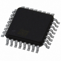
L5994 STMicroelectronics, L5994 Datasheet - Page 14

L5994
Manufacturer Part Number
L5994
Description
IC CTRLR PS ADJ TRPL-OUT 32-TQFP
Manufacturer
STMicroelectronics
Datasheet
1.L5994.pdf
(26 pages)
Specifications of L5994
Pwm Type
Current Mode
Number Of Outputs
3
Frequency - Max
345kHz
Duty Cycle
96%
Voltage - Supply
4.75 V ~ 25 V
Buck
Yes
Boost
No
Flyback
Yes
Inverting
No
Doubler
No
Divider
No
Cuk
No
Isolated
No
Operating Temperature
-40°C ~ 140°C
Package / Case
32-TQFP, 32-VQFP
Frequency-max
345kHz
Lead Free Status / RoHS Status
Lead free / RoHS Compliant
Available stocks
Company
Part Number
Manufacturer
Quantity
Price
L5994 - L5994A
Power management
The device is provided with some control pins suitable to perform some functions which are commonly used or
sometimes required in battery-operated equipment. Besides, it features controlled timing sequences in case of
turn-on/off and device shutdown for a safe and reliable behaviour under all conditions.
As above mentioned, RUN1 and RUN2 pins allow to disable separately both PWM converters by means of logic
signals (likely coming from a P) as mentioned earlier.
NOSKIP can disable the pulse-skipping feature: when it is held high neither of the PWM regulators is allowed
to enter this kind of operation.
The two PWROKx signals, one for each section, drive low immediately when the relative PWM regulator output
falls below its own undervoltage (light or hard) threshold or when it is disabled. It is high when the relative reg-
ulator runs properly.
A capacitor connected between CRST and ground fixes a time, in the order of 1.5msec/nF, which delays the
transition low-high of PWROKx. This happens at start-up of each section or after recovering an undervoltage
condition using the relative RUNx command. The delay starts from the moment in which the output voltage has
reached its correct value.
The same delay intervenes also in another circumstance: when a section is disabled (because its RUNx is driv-
en low or owing to a thermal shutdown), the relevant synchronous rectifier is turned on after the above delay in
order to make sure that the load is no longer supplied.
This delay, however, does not intervene in case of overvoltage: the synchronous rectifier is immediately turned
on after the shutdown, thus acting as a built-in "crowbar".
All these timing sequences are illustrated in fig. 7.
Design procedure
Basically, the application circuit topology is fixed, and the design procedure concerns only the selection of the
component values suitable for the voltage and current requirements of the specific application.
The design data one needs to know are therefore:
It is worth doing some preliminary considerations. The selection of the switching frequency depends on the re-
quirements of the application. If the aim is to minimize the size of the external components, 300kHz will be cho-
sen. For low input voltage applications 200kHz is preferred, since it leads to a higher maximum duty cycle.
As for the switching regulators, the inductance value of the output filter affects the inductor current ripple: the
higher the inductance the lower the ripple. This implies a lower current sense resistor value (for a given IOUT),
lower core losses and a lower output voltage ripple (for a given output capacitor) but, on the other hand, more
copper losses and a worse transient behaviour due to load changes. Usually the maximum ripple peak-to-peak
amplitude (which occurs at V
introduce a ripple factor coefficient, RF, that is therefore a number between 0.15 and 0.5.
As for the linear regulator, its input voltage VDRLIN should not fall below 12V and therefore the auxiliary wind-
ing, if used, should be dimensioned to get this voltage with a certain margin (say, 13-14V). Conversely, an high-
er input voltage leads to higher losses inside the PNP transistor, to the detriment of efficiency, and to higher
total current on the +5V inductor. Besides it implies a higher turns ratio and therefore a worse magnetic coupling,
which affect energy transfer during flyback.
14/26
Input voltage range: the minimum (V
application is expected to operate;
Maximum load current for each of the two sections;
I
I
Output voltage and current for the linear regulator, setted for 12V 50mA using an additional winding on
the 5.1V section;
Maximum peak-to-peak ripple amplitude of the output voltage for each switching section:
V
V
The operating frequency f
out1
out2
rpp1
rpp2
for the section 1;
for the section 2;
for the section 1;
for the section 2;
INMAX
SW
(200kHz / 300kHz or externally synchronized).
) is chosen between 15% and 50% of the full load current. It is convenient to
INMIN
) and the maximum (V
INMAX
) voltage under which the


