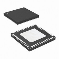
ISL9502CRZ Intersil, ISL9502CRZ Datasheet - Page 20

ISL9502CRZ
Manufacturer Part Number
ISL9502CRZ
Description
IC CTRLR PWM 2PHASE GPU 48-QFN
Manufacturer
Intersil
Datasheet
1.ISL9502CRZ-T.pdf
(24 pages)
Specifications of ISL9502CRZ
Pwm Type
Controller
Number Of Outputs
1
Frequency - Max
500kHz
Voltage - Supply
4.75 V ~ 5.25 V
Buck
Yes
Boost
No
Flyback
No
Inverting
No
Doubler
No
Divider
No
Cuk
No
Isolated
No
Operating Temperature
-10°C ~ 100°C
Package / Case
48-VQFN
Frequency-max
500kHz
Lead Free Status / RoHS Status
Lead free / RoHS Compliant
Duty Cycle
-
Therefore, the output of the droop amplifier divided by the
total load current can be expressed as follows.
where R
the temperature coefficient of the copper. To achieve the
droop value independent from the temperature of the
inductor, it is equivalently expressed by the following.
The non-inverting droop amplifier circuit has the gain
K
G
Therefore, the temperature characteristics of gain of Vn is
described by:
For the G
Rseries = 2610kΩ, and Rpar = 11kΩ, RS
generates a desired G1, close to the feature specified in
Equation 20. The actual G1 at 25°C is 0.763. For different
G1 and NTC thermistor preference, the design file to
generate the proper value of Rntc, Rseries, Rpar, and
RS
G
DCR T ( )
R
G
k
G
droopamp
droopamp
droop
1target
1
1
1
T ( )
T ( )
T ( )
EQV
•
OC
=
∆
=
=
(
is provided by Intersil.
droop
1
is the desired gain of Vn over I
=
------------------------------------------------------ -
(
VDIFF
1target
G
1
INTERNAL TO
+
------------------------------------------ -
R
ISL9502
DCR
expressed as:
=
1
+
0.00393*(T-25)
n
T ( )
0.00393*(T-25)
T ( )
1
is the realized load line slope and 0.00393 is
G
+
R
25°C
•
1t
= 0.76, the Rntc = 10kΩ with b = 4300,
+
R
--------------- -
R
n
-
+
DCR
-------------------
T ( )
arg
drp2
drp1
RS
+
+
2
•
et
10µA
EQV
(
FIGURE 26. EQUIVALENT MODEL FOR DROOP AND DIE SENSING USING DCR SENSING
25
1
+
1
1
•
)
0.00393*(T-25)
(
+
≅
)
1
+
-
-
G
+
20
RTN
1t
0.00393*(T-25)
arg
VSEN
et
DROOP
-
OUT
+
)
EQV
DROOP
OCSET
VSUM
) k
• DCR/2.
DFB
•
= 1825Ω
VO'
droopamp
(EQ. 16)
(EQ. 17)
(EQ. 18)
(EQ. 19)
(EQ. 20)
ISL9502
Cn
VSUM
Then, the individual resistors from each phase to the VSUM
node, labelled RS1 and RS2 in Figure 31, are then given by
the following equation.
So, Rs = 3650Ω. Once we know the attenuation of the RS
and RN network, we can then determine the droop amplifier
gain required to achieve the load line. Setting R
1k_1%, then R
If a droop impedance (Rdroop) = 0.0018 (V/A) is used for
example, DCR = 0.0008Ω typical for a 0.36µH inductor,
R
then given by
Note, we choose to ignore the RO resistors because they do
not add significant error.
These designed values in Rn network are very sensitive to
layout and coupling factor of the NTC to the inductor. As only
one NTC is required in this application, this NTC should be
placed as close to the Channel 1 inductor as possible and
PCB traces sensing the inductor voltage should go directly to
the inductor pads.
Once the board has been laid out, some adjustments may
be required to adjust the full load droop voltage. This is fairly
easy and can be accomplished by allowing the system to
achieve thermal equilibrium at full load, and then adjusting
R
To see whether the NTC has compensated the temperature
change of the DCR, the user can apply full load current and
wait for the thermal steady state and see how much the
Rs
Rdrp2
Rdrp2
VN
VO'
drp1
drp2
+
-
=
2 RS
= 1kΩ and the attenuation gain (G1) = 0.77, R
to obtain the appropriate load line slope.
=
=
•
⎛
⎝
⎛
⎝
----------------------------------------------- 1
DCR G1 25°C
-------------------------------------- - 1
0.0008 0.763
Rn
EQV
2 R
2 R
•
=
drp2
•
•
(
--------------------------------------------------------------------
(
droop
•
Rntc
Rntc
droop
RS
is can be found using equation
(
EQV
+
+
Vdcr
RO
Rseries
Rseries
–
)
⎞
⎠
–
=
EQV
EQV
•
RS
--------
⎞
⎠
1kΩ
2
•
)
)
=
=
R
×
+
drp1
≈
RO
-------- -
I
Rpar
Rpar
OUT
2
4.90kΩ
×
DCR
-------------
2
drp1
July 17, 2006
=
drp2
(EQ. 21)
(EQ. 22)
FN9275.1
is


