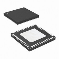
ISL9502CRZ Intersil, ISL9502CRZ Datasheet - Page 6

ISL9502CRZ
Manufacturer Part Number
ISL9502CRZ
Description
IC CTRLR PWM 2PHASE GPU 48-QFN
Manufacturer
Intersil
Datasheet
1.ISL9502CRZ-T.pdf
(24 pages)
Specifications of ISL9502CRZ
Pwm Type
Controller
Number Of Outputs
1
Frequency - Max
500kHz
Voltage - Supply
4.75 V ~ 5.25 V
Buck
Yes
Boost
No
Flyback
No
Inverting
No
Doubler
No
Divider
No
Cuk
No
Isolated
No
Operating Temperature
-10°C ~ 100°C
Package / Case
48-VQFN
Frequency-max
500kHz
Lead Free Status / RoHS Status
Lead free / RoHS Compliant
Duty Cycle
-
DROOP - Output of the droop amplifier. The voltage level on
this pin is the sum of Vo and the programmed droop voltage
by the external resistors.
DFB - Inverting input to droop amplifier.
VO - An input to the IC that reports the local output voltage.
VSUM - This pin is connected to the summing junction for
current sensing.
VIN - Supply voltage. It is used for input voltage feedforward
to improve the input line transient performance.
GND - Signal ground. Connect to local controller ground.
VDD - 5V control power supply.
ISEN2 - Individual current sharing sensing for channel 2.
ISEN1 - Individual current sharing sensing for channel 1.
NC - Not connected. Connecting this pin to the ground.
BOOT2 - Upper gate driver supply voltage for phase 2. An
internal boot strap diode is connected to the PVCC pin.
UGATE2 - Upper MOSFET gate signal for phase 2.
PHASE2 - Channel-2 phase. This pin should connect to the
source of upper MOSFET.
DROOP
VDIFF
VSUM
ISEN2
ISEN1
VSEN
GND
VDD
RTN
DFB
VIN
VO
6
ISL9502
GND PAD
(BOTTOM)
PGND2 - Return path of the lower gate driver for phase 2.
LGATE2 - Lower-side MOSFET gate signal for phase 2.
PVCC - 5V power supply for gate drivers.
LGATE1 - Lower-side MOSFET gate signal for phase 1.
PGND1 - Return path of the lower gate driver for phase 1.
PHASE1 - Channel-1 phase. This pin should connect to the
source of upper MOSFET.
UGATE1 - Upper MOSFET gate signal for phase 1.
BOOT1 - Upper gate driver supply voltage for phase 1. An
internal boot strap diode is connected to the PVCC pin.
GND - Signal ground. Connect to local controller ground.
VSEL0, VSEL1, VSEL2, VSEL3, VSEL4, VSEL5 - Voltage
selection input with VSEL0 is the least significant bit (LSB)
and VSEL5 is the most significant bit (MSB).
VR_ON - Digital input enable. A high level logic signal on
this pin enables the regulator.
SET1, SET2 - Select power-saving modes.
NC - Not connected.
GND - Signal ground. Connect to local controller ground.
GND
NC
SET2
SET1
VR_ON
VSEL5
VSEL4
VSEL3
VSEL2
VSEL1
VSEL0
GND
July 17, 2006
FN9275.1


