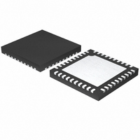
ISL6308ACRZ-T Intersil, ISL6308ACRZ-T Datasheet - Page 14

ISL6308ACRZ-T
Manufacturer Part Number
ISL6308ACRZ-T
Description
IC CTRLR PWM BUCK 3PHASE 40-QFN
Manufacturer
Intersil
Datasheet
1.ISL6308ACRZ-T.pdf
(28 pages)
Specifications of ISL6308ACRZ-T
Pwm Type
Voltage Mode
Number Of Outputs
1
Frequency - Max
275kHz
Duty Cycle
66.6%
Voltage - Supply
4.75 V ~ 5.25 V
Buck
Yes
Boost
No
Flyback
No
Inverting
No
Doubler
No
Divider
No
Cuk
No
Isolated
No
Operating Temperature
0°C ~ 70°C
Package / Case
40-VFQFN, 40-VFQFPN
Frequency-max
275kHz
Lead Free Status / RoHS Status
Lead free / RoHS Compliant
Available stocks
Company
Part Number
Manufacturer
Quantity
Price
Part Number:
ISL6308ACRZ-T
Manufacturer:
INTERSIL
Quantity:
20 000
By simply adjusting the value of R
any level, giving the converter the right amount of droop at all
load currents. It may also be necessary to compensate for any
changes in DCR due to temperature. These changes cause
the load line to be skewed, and cause the R-C time constant
to not match the L/DCR time constant. If this becomes a
problem a simple negative temperature coefficient resistor
network can be used in the place of R
for the rise in DCR due to temperature.
Output Voltage Offset Programming
The ISL6308A allows the designer to accurately adjust the
offset voltage by connecting a resistor, R
pin to VCC or GND. When R
and VCC, the voltage across it is regulated to 1.5V. This
causes a proportional current (I
and out of the FB pin. If R
voltage across it is regulated to 0.5V, and I
FB pin and out of the OFS pin. The offset current flowing
through the resistor between VDIFF and FB will generate
the desired offset voltage which is equal to the product
(I
Once the desired output offset voltage has been determined,
use the following formulas to set R
For Positive Offset (connect R
For Negative Offset (connect R
R
R
OFS
V
R
OFS
OFS
OFS
OFS
+
-
FIGURE 8. POSITIVE OFFSET OUTPUT VOLTAGE
VDIFF
x R
=
=
GND
R
I
--------------------------
V
--------------------------
V
OFS
1
1
0.5 R
1.5 R
OFS
OFFSET
OFFSET
). These functions are shown in Figures 8 and 9.
FB
⋅
⋅
PROGRAMMING
1
1
ISL6308A
VREF
OFS
OFS
14
OFS
is connected to ground, the
OFS
OFS
S
is connected between OFS
, the load line can be set to
OFS
to GND):
) to flow into the OFS pin
to VCC):
COMP
:
OFS
E/A
GND
OFS
+
to compensate
-
, from the OFS
0.5V
flows into the
VCC
(EQ. 10)
+
(EQ. 9)
-
1.5V
ISL6308A
Advanced Adaptive Zero Shoot-Through Deadtime
Control (Patent Pending)
The integrated drivers incorporate a unique adaptive
deadtime control technique to minimize deadtime, resulting
in high efficiency from the reduced freewheeling time of the
lower MOSFET body-diode conduction, and to prevent the
upper and lower MOSFETs from conducting simultaneously.
This is accomplished by ensuring either rising gate turns on
its MOSFET with minimum and sufficient delay after the
other has turned off.
During turn-off of the lower MOSFET, the PHASE voltage is
monitored until it reaches a -0.3V/+0.8V trip point for a
forward/reverse current, at which time the UGATE is
released to rise. An auto-zero comparator is used to correct
the r
detection of the -0.3V phase level during r
period. In the case of zero current, the UGATE is released
after 35ns delay of the LGATE dropping below 0.5V. During
the phase detection, the disturbance of LGATE falling
transition on the PHASE node is blanked out to prevent
falsely tripping. Once the PHASE is high, the advanced
adaptive shoot-through circuitry monitors the PHASE and
UGATE voltages during a PWM falling edge and the
subsequent UGATE turn-off. If either the UGATE falls to less
than 1.75V above the PHASE or the PHASE falls to less than
+0.8V, the LGATE is released to turn on.
Internal Bootstrap Device
All three integrated drivers feature an internal bootstrap
schottky diode. Simply adding an external capacitor across
the BOOT and PHASE pins completes the bootstrap circuit.
The bootstrap function is also designed to prevent the
bootstrap capacitor from overcharging due to the large
V
R
FIGURE 9. NEGATIVE OFFSET OUTPUT VOLTAGE
OFS
OFS
+
-
DS(ON)
VDIFF
VCC
I
OFS
R
1
OFS
FB
drop in the phase voltage preventing false
PROGRAMMING
ISL6308A
VREF
DS(ON)
E/A
GND
+
-
0.5V
September 9, 2008
conduction
VCC
FN6669.0
+
-
1.5V


