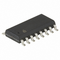
ISL6722AABZ Intersil, ISL6722AABZ Datasheet - Page 11

ISL6722AABZ
Manufacturer Part Number
ISL6722AABZ
Description
IC CTRLR PWM SGL ENDED 16-SOIC
Manufacturer
Intersil
Datasheet
1.ISL6722AAVZ.pdf
(24 pages)
Specifications of ISL6722AABZ
Pwm Type
Current Mode
Number Of Outputs
1
Frequency - Max
1MHz
Duty Cycle
100%
Voltage - Supply
9 V ~ 18 V
Buck
Yes
Boost
Yes
Flyback
Yes
Inverting
No
Doubler
No
Divider
No
Cuk
No
Isolated
Yes
Operating Temperature
-40°C ~ 105°C
Package / Case
16-SOIC (3.9mm Width)
Frequency-max
1MHz
Lead Free Status / RoHS Status
Lead free / RoHS Compliant
Available stocks
Company
Part Number
Manufacturer
Quantity
Price
Part Number:
ISL6722AABZ
Manufacturer:
INTERSIL
Quantity:
20 000
Part Number:
ISL6722AABZ-T
Manufacturer:
INTERS
Quantity:
20 000
The minimum amount of slope compensation required
corresponds to 1/2 the inductor downslope. However, adding
excessive slope compensation results in a control loop that
behaves more as a voltage mode controller than as current
mode controller.
The minimum amount of capacitance to place at the SLOPE
pin is:
Cslope
where t
voltage to be added as slope compensation to the current
feedback signal. In general, the amount of slope
compensation added is 2 to 3 times the minimum required.
Example:
Assume the inductor current signal presented at the ISENSE
pin decreases 125mV during the Off period, and:
Switching Frequency, f
Duty Cycle, D = 60%
t
t
Determine the downslope:
Downslope = 0.125V/1.6µs = 78mV/µs. Now determine the
amount of voltage that must be added to the current sense
signal by the end of the On time.
Vslope
Therefore,
Cslope min
The value calculated, 110pF, represents the minimum slope
compensation required. An appropriate slope compensation
capacitance for this example would be 1/2 to 1/3 the
calculated value, or between 68pF and 33pF.
A more rigorous treatment of slope compensation can be
obtained from the small signal current-mode model [1]. It can
ON
OFF
= D/f
= (1 - D)/f
(
ON
CURRENT SENSE SIGNAL
=
=
sw
Current Sense Signal
1
-- - 0.078 2.4
2
4.24
is the On time and Vslope is the amount of
•
)
= 0.6/250E3 = 2.4µs
=
×10
sw
4.24
–
= 1.6µs
6
•
×10
•
------------------- -
Vslope
sw
–
t
ON
6
=
•
FIGURE 5.
= 250kHz
94mV
2.4
-----------------------
TIME
0.094
11
Time
×10
DOWNSLOPE
–
F
Downslope
6
≈
110pF
ISL6722A, ISL6723A
(EQ. 6)
(EQ. 7)
(EQ. 8)
be shown that the naturally-sampled modulator gain, Fm,
without slope compensation, is Equation 9:
Fm
where Sn is the slope of the sawtooth signal and t
switching frequency. When an external ramp is added, the
modulator gain becomes Equation 10:
Fm
where Se is slope of the external ramp.
m
The criteria for determining the correct amount of external
ramp can be determined by appropriately setting the
damping factor of the double-pole located at half the
oscillator frequency. The double-pole will be critically
damped if the Q-factor is set to 1, under-damped for Q > 1,
and over-damped for Q < 1. An under-damped condition
may result in current loop instability.
Q
where D is the maximum duty cycle. Setting Q = 1 and
solving for S
S
Since S
and the external ramp, respectively, they can be multiplied
by t
V
where V
the on time and V
external ramp.
For buck-derived topologies, V
output voltage, current transducer components, and output
inductance yielding:
V
where R
current transformer turns ratio, L
V
and primary turns, respectively.
e
e
e
O
c
=
=
=
=
=
ON
is the output voltage, and N
=
=
-------------------------------------------------
π m
S
V
t
--------------------------------------- -
1
(
-------------------- -
Sn t
----------------------------------- -
(
SW
n
n
Sn
to obtain the voltage change that occurs during t
+
n
⎛
⎝
⎛
⎝
n
N
CS
c
Se
-------
Sn
⎛
⎝
⎛
⎝
1
⋅
and S
(
⋅
CT
1
-- -
π
1
-- -
π
is the change in the current feedback signal during
+
1 D
V
sw
+
+
1
Se
is the current sense burden resistor, N
–
O
1
e
⋅
0.5
0.5
L
⋅
yields:
)t
R
O
) 0.5
e
⎞
⎠
⎞
⎠
sw
–
CS
------------ - 1
1 D
------------ - 1
1 D
are the on time slopes of the current ramp
e
–
–
1
1
=
is the voltage that must be added by the
⋅
)
N
------- -
N
------------------------ -
m
S
P
–
–
c
⎛
⎝
Snt
1
-- -
π
⎞
⎠
⎞
⎠
1
+
sw
D 0.5
–
n
s
can be solved for in terms of
O
and N
⎞
⎠
is the output inductance,
p
V
are the secondary
sw
CT
July 11, 2007
(EQ. 12)
(EQ. 14)
(EQ. 15)
is the
(EQ. 10)
(EQ. 11)
(EQ. 13)
is the
FN9237.1
(EQ. 9)
ON
.


