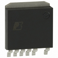
DPA426SN Power Integrations, DPA426SN Datasheet - Page 15

DPA426SN
Manufacturer Part Number
DPA426SN
Description
IC CONV DC-DC DPA SWITCH SPAK
Manufacturer
Power Integrations
Series
DPA-Switch®r
Specifications of DPA426SN
Applications
Converter, Power Over Ethernet and Telecom Applications
Voltage - Input
16 ~ 75 V
Number Of Outputs
1
Voltage - Output
220V
Operating Temperature
-40°C ~ 125°C
Mounting Type
Surface Mount
Package / Case
SPak (5 leads + Tab)
Mounting Style
SMD/SMT
Lead Free Status / RoHS Status
Lead free / RoHS Compliant
Available stocks
Company
Part Number
Manufacturer
Quantity
Price
Company:
Part Number:
DPA426SN
Manufacturer:
POWER
Quantity:
15 000
Part Number:
DPA426SN
Manufacturer:
POWER
Quantity:
20 000
Part Number:
DPA426SN-TL
Manufacturer:
POWER
Quantity:
20 000
Figure 12. Synchronous Rectification (a) Winding Driven DC
output. For a 5 V output, an efficiency of 85% with Schottky
rectifiers would typically go to 90% or higher with synchronous
rectifiers. Synchronous rectification gives the benefit of greater
efficiency at lower output voltages as shown in Table 3.
DPA-Switch has features that can simplify the design of
synchronous rectifier circuits that are in common use. Circuits
for synchronous rectification with DPA-Switch fall into three
categories of increasing complexity.
a) Winding Driven DC Coupled
b) Winding Driven AC Coupled
c) Actively Driven
The first two are shown in Figures 11 and 12. MOSFETs Q1
and Q2 conduct at appropriate times to reduce the voltage drops
associated with the output rectifiers of a forward converter. Q2
performs the function of the forward rectifier. Q1 operates as the
catch rectifier with a parallel Schottky diode. The voltage drop
of each synchronous rectifier is dominated by the on-resistance
of the MOSFETs multiplied by the RMS load current, rather
than by the average current times the minimum voltage of a
Schottky barrier.
Winding Driven DC Coupled Synchronous Rectifier
The simplest way to drive synchronous rectifiers with
DPA-Switch is shown in Figure 12 (a). The gate-to-source
voltage that turns on the MOSFETs is essentially the voltage
at the secondary winding of the transformer. The channel of the
MOSFET will conduct as long as the gate-to-source voltage
exceeds the threshold voltage.
Coupled. (b) Winding Driven AC Coupled.
R15
Q2
Q2
R15
R16
C17
(a)
(b)
Q1
D4
Q1
D3
PI-2989-062204
PI-3475-062204
D3
L2
L2
Table 3. Efficiency Gain vs. Output Voltage for Synchronous
The forward rectifier MOSFET Q2 turns on when the
DPA-Switch turns on to apply the DC input voltage across the
primary winding. The direction of current in Q2 is from source
to drain. When the DPA-Switch turns off, the reset voltage on
the transformer forces a negative gate-to-source voltage on Q2
and a positive gate-to-source voltage on Q1. Schottky diode D3
conducts until the gate-to-source voltage on Q1 rises sufficiently
to exceed the threshold voltage.
Suitable MOSFETs for this application have threshold voltages
typically between 4 V and 5 V. The permissible maximum gate-
to-source voltage is usually 15 V to 20 V. These restrictions
limit the range of input voltage for converter operation.
The integrated line overvoltage feature of DPA-Switch simplifies
the design of winding driven synchronous rectifiers. In most
cases it eliminates the need for Zener diodes to protect the gates
of the MOSFETs from excessive voltage. Excess voltage will
not appear on the secondary of the transformer because the
DPA-Switch will not operate when the input voltage is too
high.
DC coupling of the gates in this configuration permits a mode
of operation that may not be desirable in some applications.
During shutdown, the voltage across the output inductor will go
to zero after its current decays to zero. The remaining output
voltage will then appear across Q1 and D3.
If the output voltage is high enough (above the gate threshold
of Q2) it will turn on Q2, allowing reverse current to flow
through L2 and the transformer secondary. The voltage on the
secondary winding will saturate the transformer, abruptly turning
off Q2 and generating a voltage spike on the gate of Q1. This
voltage spike may exceed the rated gate voltage for Q1. This
behavior can occur in any design using this form of synchronous
rectification with an undervoltage lockout. It is not specific to
DPA-Switch. A solution to this issue is offered below.
Winding Driven AC Coupled Synchronous Rectifier
The AC coupled circuit of Figure 12 (b) eliminates the high
voltage spike by limiting the on-time of Q2 such that significant
reverse current cannot flow through L2 and the secondary
Output Voltage
Rectification.
3.3 V
2.5 V
5 V
Efficiency Gain Over Diode
Rectification
+3%
+6%
+8%
AN-31
7/04
C
15


