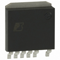
DPA426SN Power Integrations, DPA426SN Datasheet - Page 16

DPA426SN
Manufacturer Part Number
DPA426SN
Description
IC CONV DC-DC DPA SWITCH SPAK
Manufacturer
Power Integrations
Series
DPA-Switch®r
Specifications of DPA426SN
Applications
Converter, Power Over Ethernet and Telecom Applications
Voltage - Input
16 ~ 75 V
Number Of Outputs
1
Voltage - Output
220V
Operating Temperature
-40°C ~ 125°C
Mounting Type
Surface Mount
Package / Case
SPak (5 leads + Tab)
Mounting Style
SMD/SMT
Lead Free Status / RoHS Status
Lead free / RoHS Compliant
Available stocks
Company
Part Number
Manufacturer
Quantity
Price
Company:
Part Number:
DPA426SN
Manufacturer:
POWER
Quantity:
15 000
Part Number:
DPA426SN
Manufacturer:
POWER
Quantity:
20 000
Part Number:
DPA426SN-TL
Manufacturer:
POWER
Quantity:
20 000
winding. Capacitor C17 should be chosen to capacitively divide
the winding voltage between C17 and the C
Q2, to provide a voltage on C
voltage. The time constant of C17 and R16 should be about
10 µs for 300 kHz operation. R15 is typically about 10 Ω.
Figure 11 shows the DPA-Switch in a single-ended DC-DC
forward converter that uses winding driven AC coupled
synchronous rectification. In this example, the gate of Q1
has enough capacitance to eliminate the need for the discrete
capacitor C
is often the case with synchronous rectifiers that are winding
driven, designers should follow the guidance in the section on
Verification of Transformer Reset to confirm that the transformer
resets properly.
Actively Driven Synchronous Rectifiers
The third category of synchronous rectifier circuits uses
independent active components that may include discrete devices
and integrated circuits to lock onto the switching frequency of
the power supply and to drive the MOSFETs. This solution
relaxes the restriction on the range of input voltage because the
driver can regulate the gate voltage to be independent of the
voltage on the secondary winding. Circuits for actively driven
synchronous rectifiers are much more complex than the other
solutions, and are beyond the scope of this application note.
Table 4 gives a comparison of the techniques for synchronous
rectification.
In general, DPA-Switch with synchronous rectifiers should
operate at the lower switching frequency of 300 kHz. The
synchronous rectifier catch MOSFETs typically have gate-
source capacitance values such that the transformer would have
insufficient time to reset at 400 kHz. Connect the F pin to the
CONTROL pin to select the lower switching frequency.
Layout Considerations
Figure 13 shows an example of a proper circuit board layout for
a forward converter with DPA-Switch. Since the DPA-Switch
can operate with large drain current, designers should follow
these guidelines carefully.
Table 4. Comparison of Synchronous Rectification Techniques.
16
Synchronous Rectifier Type
Winding Driven DC Coupled
Winding Driven AC Coupled
C
7/04
AN-31
S
in the transformer reset circuit. Although this
Active Drive
GS
that exceeds the Q2 threshold
GS
Efficiency
of MOSFET
⇑
⇑
⇑
Complexity
and Cost
Primary Side Connections
The tab of DPA-Switch is the intended return connection for the
high switching currents. Therefore, the tab should be connected
by wide, low impedance traces to the input capacitor. The
SOURCE pin should not be used to return the power currents;
incorrect operation of the device may result. The SOURCE pin
is intended as a signal ground only. The device tab (SOURCE)
is the correct connection for power currents.
The bypass capacitor on the CONTROL pin should be located
as close as possible to the SOURCE and CONTROL pins. The
circuit trace of its connection to SOURCE should not contain
any switching current from the primary or bias voltages.
All SOURCE pin referenced components connected to the
LINE-SENSE (L) or EXTERNAL CURRENT LIMIT (X)
pins should also be located closely between their respective
pins and SOURCE. Once again, the SOURCE connection
trace of these components should not conduct any of the main
MOSFET switching currents. It is critical that tab (SOURCE)
power switching currents are returned to the negative terminal
of the input capacitor through a separate trace that is not shared
by the components connected to the SOURCE, CONTROL,
L or X pins.
Any traces to the L or X pins should be kept as short as possible
and away from the drain trace to prevent noise coupling. Line-
sense resistor (R1 in Figure 11) should be located close to the L
pin to minimize the trace length on the L pin side. In addition
to the CONTROL pin capacitor (C5 in Figure 11), a 220 nF
high frequency bypass capacitor in parallel is recommended
as close as possible between SOURCE and CONTROL pins
for better noise immunity. The feedback optocoupler output
should also be located close to the CONTROL and SOURCE
pins of DPA-Switch.
Heat Sinking
To maximize heat sinking of the DPA-Switch and the other
power components, special thermally conductive PC board
material (aluminum clad PC board) is recommended. This
has an aluminum sheet bonded to the PC board during the
manufacturing process to provide heat sinking directly or to
allow the attachment of an external heat sink. If normal PC
⇑⇑⇑
⇔
⇓
Gate Voltage Controlled at Power Down
Check Gate Voltage at Power Down
High Complexity
Comment


