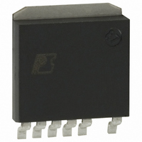
DPA426SN Power Integrations, DPA426SN Datasheet - Page 8

DPA426SN
Manufacturer Part Number
DPA426SN
Description
IC CONV DC-DC DPA SWITCH SPAK
Manufacturer
Power Integrations
Series
DPA-Switch®r
Specifications of DPA426SN
Applications
Converter, Power Over Ethernet and Telecom Applications
Voltage - Input
16 ~ 75 V
Number Of Outputs
1
Voltage - Output
220V
Operating Temperature
-40°C ~ 125°C
Mounting Type
Surface Mount
Package / Case
SPak (5 leads + Tab)
Mounting Style
SMD/SMT
Lead Free Status / RoHS Status
Lead free / RoHS Compliant
Available stocks
Company
Part Number
Manufacturer
Quantity
Price
Company:
Part Number:
DPA426SN
Manufacturer:
POWER
Quantity:
15 000
Part Number:
DPA426SN
Manufacturer:
POWER
Quantity:
20 000
Part Number:
DPA426SN-TL
Manufacturer:
POWER
Quantity:
20 000
Figure 6. A 70 W DC-DC Converter that uses an Alternative Circuit to Reset the Transformer.
balance and prevent saturation. Since real transformers have
finite inductance, they store parasitic energy that is represented
as a magnetizing current.
The magnetizing inductance cannot store very much energy
before it saturates. Since a saturated transformer behaves like
a short circuit, external circuitry must manage the removal
of the energy from the magnetization inductance (reset the
transformer) on each switching cycle.
This transformer reset will require the voltage on the DRAIN
pin to rise above the input voltage. The designer needs to be
sure that the transformer reset does not cause voltage overstress
on the DRAIN pin of the DPA-Switch.
Figure 4 shows the components for the circuit that resets the
magnetizing energy in the transformer to a safe value at the
end of each switching cycle. The heart of the circuit is the
series RC network (R
output rectifier.
When the DPA-Switch turns off, current in the magnetizing
inductance leaves the transformer through the secondary
winding. The capacitor charges as the magnetizing current
reduces to zero. The capacitor must be small enough to allow
the magnetizing current to go to zero within the minimum
offtime. An additional restriction on the size of the capacitor is
that it must be large enough to keep the drain-to-source voltage
below the voltage of the Zener clamp under normal operating
8
INPUT RTN
36-72 VDC
J1-2
100 V
+V
J1-1
1 µF
C1
IN
C
7/04
AN-31
100 V
1 µF
C2
2.5 A
1 µH
L1
100 V (x4)
C3, C4,
C5, C6
1 µF,
S
SMBJ
100 µH
VR1
UF4003
150
and C
L2
D2
UF4003
D1
470 pF
200 V
S
C8
) that is connected across the
D
S
CONTROL
CONTROL
X
L
619 kΩ
F
R1
6.8 kΩ
C
1 %
R3
DPA-Switch
U1
DPA426R
220 nF
C10
2
1
3
1.5 kV
1 nF
C7
9, 10
T1
6, 7
68 µF
1.0 Ω
10 V
C11
6.8 Ω
R4
R5
4.7 nF
50 V
C12
6.8 Ω
R6
PC357N3T
conditions. The resistor in the reset network damps oscillations
from the interaction of the capacitor with parasitic inductance.
The value of the resistor is typically between 1 Ω and 5 Ω.
A different reset circuit is required for applications higher than
about 40 W. Figure 6 shows an example of a 70 W converter
that uses the circuit of Figure 5 to reset the transformer and to
limit the voltage on the DPA-Switch.
Verification of Transformer Reset
Users should confirm that the transformer resets under worst
case conditions at the lowest and highest input voltages with
measurements on the bench. Figure 7 illustrates three situations
that show proper transformer reset with the reset circuit in
Figure 4. Three examples of improper transformer reset are
shown in Figure 8.
The best way to assess the reset characteristics is to observe the
drain-to-source voltage on the DPA-Switch. Figure 7 (a) shows
the voltage on the prototype example when it operates from an
input of 72 VDC. It is operating at full load with a reset capacitor
(C
on the primary is 47 pF. See Design Idea DI-24 (available on
www.powerint.com) for a circuit example.
The figure shows the important intervals of the waveform
within one switching period T
during the time t
42CT030S
U2
BAV19
WS
42CT030S
D3
S
D4
) of 2.2 nF across the output rectifier. The clamp capacitor
D5
4.7 µF
25 V
C9
3.3 µH
20 A
ON
L3
= D T
C15, C16, C17
C13, C14,
10 V (x5)
100 µF,
S
, where D is the duty ratio. Flux in
10 kΩ
BAV19WS
10 µF
LM431AIM3
R8
10 V
C21
100 nH
D5
20 A
220 Ω
U3
S
L4
R10
. DPA-Switch is conducting
U2
100 µF
10 V
C18
1 µF
C22
5.1 Ω
68 nF
R11
C23
100 µF
10 V
C19
10.0 kΩ
10.0 kΩ
R13
220 Ω
1%
R14
1%
R9
1 µF
10 V
C20
PI-2882-062204
5 V, 14 A
J2-2
J1-1
RTN


