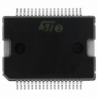
L6701TR STMicroelectronics, L6701TR Datasheet - Page 21

L6701TR
Manufacturer Part Number
L6701TR
Description
IC CTRLR 3PH VR10/9/K8 PWRSSO-36
Manufacturer
STMicroelectronics
Datasheet
1.L6701TR.pdf
(44 pages)
Specifications of L6701TR
Applications
Controller, Intel VR9, VR10, K8
Voltage - Input
12V
Number Of Outputs
3
Voltage - Output
0.8 ~ 1.85 V
Operating Temperature
0°C ~ 70°C
Mounting Type
Surface Mount
Package / Case
36-PowerSOIC
Output Voltage
0.8 V to 1.85 V
Output Current
1.5 A
Switching Frequency
110 KHz
Mounting Style
SMD/SMT
Maximum Operating Temperature
+ 125 C
Minimum Operating Temperature
0 C
Lead Free Status / RoHS Status
Lead free / RoHS Compliant
Other names
497-6108-2
L6701
10
10.1
Output Voltage Positioning
Output voltage positioning is performed by selecting the reference DAC and by programming
the Droop Function and Offset to the reference (See
from the FB pin, directly proportional to the read current, causes the output voltage to vary
according to the external R
current (I
to the resistance R
The output voltage is then driven by the following relationship:
Both DROOP and OFFSET function can be disabled: see
details.
Figure 7.
Load-Line (Droop Function - Optional)
This method "recovers" part of the drop due to the output capacitor ESR in the load transient,
introducing a dependence of the output voltage on the load current: a static error proportional to
the output current causes the output voltage to vary according to the sensed current.
Figure 8
cost application (saves component count). The current flowing across the three inductors is
read through the R
gain and generates a current I
phases. The current I
(I
Considering the scheme reported on
Time constant matching between the inductor (L / DCR) and the current reading filter
(
avoiding over and/or under shoot of the output voltage as a consequence of a load transient. It
results:
R
DROOP
PH
⋅
C
PH
). R
OS
shows the typical Current-Sense Circuit used to implement the Droop-Function in low-
3 ⁄
) sourced from the REF_IN pin causes the reference voltage to be offset according
FB
VID
Voltage Positioning
) is required to implement a real equivalent output impedance of the system so
REF_OUT
gives the final gain to program the desired load-line slope.
FB
PH
CS
connected.
R
C
- C
OS
OS
is then mirrored and, multiplied by three, sourced by the FB pin
PH
REF_IN
V
FB
I
CS
O UT
filter across CS+ and CS- pins. R
resistor so implementing the desired load-line resistance. The
CS
=
=
proportional to the average of the currents of the three
I
------------
O UT
VID
3
FB
Figure
⋅
+
--------------------------------------------------- -
1
R
+
1
O S
R
8, it is possible to observe that:
R
s R
FB
+
F
⋅
s L
⋅
I
⋅
PH
O S
COMP
C
⁄
F
⋅
–
DCR
Figure
C
R
PH
FB
VSEN
Section 10.1
3 ⁄
⋅
7). The current (I
I
DRO OP
⋅
D
DCR
------------ -
R
programs a trans-conductance
D
10 Output Voltage Positioning
64k
64k
and
FBR
(Remote Sense)
Section 10.3
To Vcore
DROOP
FBG
) sourced
for
21/44


