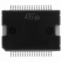
L6701TR STMicroelectronics, L6701TR Datasheet - Page 7

L6701TR
Manufacturer Part Number
L6701TR
Description
IC CTRLR 3PH VR10/9/K8 PWRSSO-36
Manufacturer
STMicroelectronics
Datasheet
1.L6701TR.pdf
(44 pages)
Specifications of L6701TR
Applications
Controller, Intel VR9, VR10, K8
Voltage - Input
12V
Number Of Outputs
3
Voltage - Output
0.8 ~ 1.85 V
Operating Temperature
0°C ~ 70°C
Mounting Type
Surface Mount
Package / Case
36-PowerSOIC
Output Voltage
0.8 V to 1.85 V
Output Current
1.5 A
Switching Frequency
110 KHz
Mounting Style
SMD/SMT
Maximum Operating Temperature
+ 125 C
Minimum Operating Temperature
0 C
Lead Free Status / RoHS Status
Lead free / RoHS Compliant
Other names
497-6108-2
L6701
Table 1.
21 to 26
29 to 31
Pin n
PAD
19
20
27
28
32
33
34
35
36
°
Pins description (continued)
VID0, VID5
THERMAL
REF_OUT
REF_IN
ISEN3
ISEN1
COMP
Name
VSEN
VID4
FBR
FBG
CS+
PAD
CS-
FB
to
to
Reference Input for the regulation.
Connect directly or through a resistor to the REF_OUT pin. See
details. This pin is used as input for the protections.
Reference Output.
Connect directly or through a resistor to the REF_IN pin. See
details.
Voltage IDentification Pins.
Internally pulled up by 12.5µA to 5V, connect to SGND to program a '0' or leave
floating to program a '1'. They allow programming output voltage as specified in
Table
Remote Buffer Non Inverting Input.
Connect to the positive side of the load to perform remote sense.
See
Remote Buffer Inverting Input.
Connect to the negative side of the load to perform remote sense.
See
LS Current Sense Pins.
These pins are used for current balance phase-to-phase as well as for the
system OCP. Connect through a resistor R
Section 9
Droop Current Sense non-inverting input.
Connect through R
output voltage when Droop function is not required. See
Section 10.2
Droop Current Sense inverting input.
Connect through resistor R
when Droop Function is not required. See
details.
This pin also monitors the output for any feedback disconnection. See
Section 13.4
Remote Buffer Output. It manages OVP and UVP protections and PGOOD
(when applicable). See
Error Amplifier Inverting Input. Connect with a resistor R
R
Error Amplifier Output. Connect with an R
The device cannot be disabled by pulling down this pin.
Thermal pad connects the Silicon substrate and makes good thermal contact
with the PCB to dissipate the power necessary to drive the external MOSFETs.
Connect to the PGND plane with several VIAs to improve thermal conductivity.
F
- C
Section 16
Section 16
5,
F
toward COMP.
Table 6
and
for details.
for details.
Section 13.6
for proper layout of this connection.
for proper layout of this connection.
and
PH
Table 7
-C
Section 13
PH
network to the main inductors. Directly connect to
D
for details.
to the main inductors common node. Leave floating
according to DAC_SEL status.
for details.
Function
2 Pins description and connection diagrams
F
Section 10.1
ISEN
- C
F
to the relative PHASEx pin. See
vs. FB.
FB
and
Section 10.1
vs. VSEN and with an
Section 10.2
Section 10.3
Section 10.3
and
for
for
7/44
for


