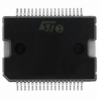
L6701TR STMicroelectronics, L6701TR Datasheet - Page 37

L6701TR
Manufacturer Part Number
L6701TR
Description
IC CTRLR 3PH VR10/9/K8 PWRSSO-36
Manufacturer
STMicroelectronics
Datasheet
1.L6701TR.pdf
(44 pages)
Specifications of L6701TR
Applications
Controller, Intel VR9, VR10, K8
Voltage - Input
12V
Number Of Outputs
3
Voltage - Output
0.8 ~ 1.85 V
Operating Temperature
0°C ~ 70°C
Mounting Type
Surface Mount
Package / Case
36-PowerSOIC
Output Voltage
0.8 V to 1.85 V
Output Current
1.5 A
Switching Frequency
110 KHz
Mounting Style
SMD/SMT
Maximum Operating Temperature
+ 125 C
Minimum Operating Temperature
0 C
Lead Free Status / RoHS Status
Lead free / RoHS Compliant
Other names
497-6108-2
L6701
15.1
Compensation Network Guidelines
The Compensation Network design assures to having system response according to the cross-
over frequency selected and to the output filter considered: it is anyway possible to further fine-
tune the compensation network modifying the bandwidth in order to get the best response of
the system as follow (See
Having the fastest compensation network gives not the confidence to satisfy the requirements
of the load: the inductor still limits the maximum dI/dt that the system can afford. In fact, when a
load transient is applied, the best that the controller can do is to “saturate” the duty cycle to its
maximum (d
charge / discharge time and by the output capacitance. In particular, the most limiting transition
corresponds to the load removal since the inductor results being discharged only by V
(while it is charged by d
Referring to
improvements unless the output filter changes: only modifying the main inductors or the output
capacitance improves the system response.
Figure 19. Best Load Transient achievable (d=0) and R
Increase R
Decrease R
Increase C
phase margin.
MAX
Figure
F
F
) or minimum (0) value. The output voltage dV/dt is then limited by the inductor
F
to increase the system bandwidth accordingly;
to move ω
to decrease the system bandwidth accordingly;
19-left, further tuning the Compensation network cannot give any
MAX
Figure
V
F
IN
to low frequencies increasing as a consequence the system
-V
OUT
19):
during a load appliance).
R
F
[dB]
K
dB
15 System Control Loop Compensation
F
ω
-C
LC
C
=
F
F
G
ω
impact on Bandwidth.
F
LOOP
ω
ESR
(s)
ω
T
R
F
Z
ω
F
(s)
OUT
37/44


