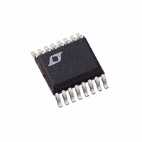
LTC3703EGN Linear Technology, LTC3703EGN Datasheet - Page 16

LTC3703EGN
Manufacturer Part Number
LTC3703EGN
Description
IC BUCK/BOOST SYNC ADJ 5A 16SSOP
Manufacturer
Linear Technology
Type
Step-Down (Buck), Step-Up (Boost)r
Datasheet
1.LTC3703EGNPBF.pdf
(32 pages)
Specifications of LTC3703EGN
Internal Switch(s)
No
Synchronous Rectifier
Yes
Number Of Outputs
1
Voltage - Output
0.8 ~ 93 V
Current - Output
5A
Frequency - Switching
100kHz ~ 600kHz
Voltage - Input
9.3 ~ 100 V
Operating Temperature
-40°C ~ 85°C
Mounting Type
Surface Mount
Package / Case
16-SSOP
Lead Free Status / RoHS Status
Contains lead / RoHS non-compliant
Power - Output
-
Available stocks
Company
Part Number
Manufacturer
Quantity
Price
Company:
Part Number:
LTC3703EGN
Manufacturer:
LINEAR
Quantity:
4
Part Number:
LTC3703EGN
Manufacturer:
LTNEAR
Quantity:
20 000
Company:
Part Number:
LTC3703EGN#PBF
Manufacturer:
LT
Quantity:
3 291
Part Number:
LTC3703EGN#PBF
Manufacturer:
LINEAR/凌特
Quantity:
20 000
Company:
Part Number:
LTC3703EGN#TRPBF
Manufacturer:
LT
Quantity:
3 291
Part Number:
LTC3703EGN#TRPBF
Manufacturer:
LTNEAR
Quantity:
20 000
Company:
Part Number:
LTC3703EGN-5
Manufacturer:
LT
Quantity:
10 000
Part Number:
LTC3703EGN-5
Manufacturer:
LINEAR/凌特
Quantity:
20 000
Company:
Part Number:
LTC3703EGN-5#PBF
Manufacturer:
LT
Quantity:
320
Part Number:
LTC3703EGN-5#PBF
Manufacturer:
LINEAR/凌特
Quantity:
20 000
APPLICATIONS INFORMATION
LTC3703
Since ΔI
is highest at maximum input voltage. ESR also has a
signifi cant effect on the load transient response. Fast load
transitions at the output will appear as voltage across the
ESR of C
change the inductor current to match the new load current
value. Typically, once the ESR requirement is satisfi ed the
capacitance is adequate for fi ltering and has the required
RMS current rating.
Manufacturers such as Nichicon, Nippon Chemi-Con and
Sanyo should be considered for high performance through-
hole capacitors. The OS-CON (organic semiconductor
dielectric) capacitor available from Sanyo has the lowest
product of ESR and size of any aluminum electrolytic at
a somewhat higher price. An additional ceramic capacitor
in parallel with OS-CON capacitors is recommended to
reduce the effect of their lead inductance.
In surface mount applications, multiple capacitors placed
in parallel may be required to meet the ESR, RMS current
handling and load step requirements. Dry tantalum, special
polymer and aluminum electrolytic capacitors are available
in surface mount packages. Special polymer capacitors
offer very low ESR but have lower capacitance density
than other types. Tantalum capacitors have the highest
capacitance density but it is important to only use types
that have been surge tested for use in switching power
supplies. Several excellent surge-tested choices are the
AVX TPS and TPSV or the KEMET T510 series. Aluminum
electrolytic capacitors have signifi cantly higher ESR, but
can be used in cost-driven applications providing that
consideration is given to ripple current ratings and long
term reliability. Other capacitor types include Panasonic
SP and Sanyo POSCAPs.
Output Voltage
The LTC3703 output voltage is set by a resistor divider
according to the following formula:
The external resistor divider is connected to the output as
shown in the Functional Diagram, allowing remote voltage
16
V
OUT
L
=
OUT
increases with input voltage, the output ripple
0 8
.
until the feedback loop in the LTC3703 can
V
⎛
⎝ ⎜
1
+
R
R
2
1
⎞
⎠ ⎟
sensing. The resultant feedback signal is compared with
the internal precision 800mV voltage reference by the
error amplifi er. The internal reference has a guaranteed
tolerance of ±1%. Tolerance of the feedback resistors will
add additional error to the output voltage. 0.1% to 1%
resistors are recommended.
MOSFET Driver Supplies (DRV
The LTC3703 drivers are supplied from the DRV
BOOST pins (see Figure 3), which have an absolute
maximum voltage of 15V. If the main supply voltage,
V
between 9V and 15V must be used to power the drivers.
If a separate supply is not available, one can easily be
generated from the main supply using one of the circuits
shown in Figure 10. If the output voltage is between 10V
and 15V, the output can be used to directly power the
drivers as shown in Figure 10a. If the output is below 10V,
Figure 10b shows an easy way to boost the supply voltage
to a suffi cient level. This boost circuit uses the LT1613
in a ThinSOT ™ package and a chip inductor for minimal
extra area (<0.2in
extra winding on the inductor (Figure 10c) or a capaci-
tive charge pump (Figure 10d). All the circuits shown in
Figure 10 require a start-up circuit (Q1, D1 and R1) to
provide driver power at initial start-up or following a short-
circuit. The resistor R1 must be sized so that it supplies
suffi cient base current and zener bias current at the lowest
expected value of V
supply must be capable of supplying the required gate
driver current which can be estimated from:
This equation for I
the circuit components shown in Figure 10.
An external bootstrap capacitor, C
BOOST pin supplies the gate drive voltage for the topside
MOSFETs. Capacitor C
D
topside MOSFET is turned on, the driver places the C
voltage across the gate source of the top MOSFET. The
switch node voltage, SW, rises to V
follows. With the topside MOSFET on, the boost voltage
ThinSOT is a trademark of Linear Technology Corporation.
IN
B
I
, from the DRV
, is higher than 15V a separate supply with a voltage
DRVCC
= (f)(Q
G(TOP)
2
DRVCC
CC
). Two other possible schemes are an
IN
. When using an existing supply, the
supply when SW is low. When the
B
+ Q
is charged through external diode,
is also useful for properly sizing
G(BOTTOM)
CC
and BOOST)
IN
B
)
, connected to the
and the BOOST pin
CC
3703fb
and
B


