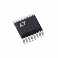
LTC3703EGN Linear Technology, LTC3703EGN Datasheet - Page 8

LTC3703EGN
Manufacturer Part Number
LTC3703EGN
Description
IC BUCK/BOOST SYNC ADJ 5A 16SSOP
Manufacturer
Linear Technology
Type
Step-Down (Buck), Step-Up (Boost)r
Datasheet
1.LTC3703EGNPBF.pdf
(32 pages)
Specifications of LTC3703EGN
Internal Switch(s)
No
Synchronous Rectifier
Yes
Number Of Outputs
1
Voltage - Output
0.8 ~ 93 V
Current - Output
5A
Frequency - Switching
100kHz ~ 600kHz
Voltage - Input
9.3 ~ 100 V
Operating Temperature
-40°C ~ 85°C
Mounting Type
Surface Mount
Package / Case
16-SSOP
Lead Free Status / RoHS Status
Contains lead / RoHS non-compliant
Power - Output
-
Available stocks
Company
Part Number
Manufacturer
Quantity
Price
Company:
Part Number:
LTC3703EGN
Manufacturer:
LINEAR
Quantity:
4
Part Number:
LTC3703EGN
Manufacturer:
LTNEAR
Quantity:
20 000
Company:
Part Number:
LTC3703EGN#PBF
Manufacturer:
LT
Quantity:
3 291
Part Number:
LTC3703EGN#PBF
Manufacturer:
LINEAR/凌特
Quantity:
20 000
Company:
Part Number:
LTC3703EGN#TRPBF
Manufacturer:
LT
Quantity:
3 291
Part Number:
LTC3703EGN#TRPBF
Manufacturer:
LTNEAR
Quantity:
20 000
Company:
Part Number:
LTC3703EGN-5
Manufacturer:
LT
Quantity:
10 000
Part Number:
LTC3703EGN-5
Manufacturer:
LINEAR/凌特
Quantity:
20 000
Company:
Part Number:
LTC3703EGN-5#PBF
Manufacturer:
LT
Quantity:
320
Part Number:
LTC3703EGN-5#PBF
Manufacturer:
LINEAR/凌特
Quantity:
20 000
LTC3703
FUNCTIONAL DIAGRAM
The LTC3703 is a constant frequency, voltage mode con-
troller for DC/DC step-down converters. It is designed to
be used in a synchronous switching architecture with two
external N-channel MOSFETs. Its high operating voltage
capability allows it to directly step down input voltages up
to 100V without the need for a step-down transformer. For
circuit operation, please refer to the Functional Diagram
OPERATION
8
R2
R1
V
C
CC
SS
C
16
12
VCC
5
1
3
4
MODE/SYNC
0.8V
RUN/SS
COMP
FB
V
3.2V
V
(<15V)
GN16
IN
CC
(Refer to Functional Diagram)
+
+
–
OVER
TEMP
OT SD
FB
0.9V
4μA
+
–
÷
DETECT
SYNC
UVSD OTSD
REFERENCE
BANDGAP
0.8V
% DC
LIMIT
EXT SYNC
FORCED CONTINUOUS
+
CHIP
SD
–
PWM
INTERNAL
3.2V V
OSC
0.76V
2
V
+
f
MIN
CC
SET
R
CC
–
SET
0.84V
+
MAX
–
UVLO
UV SD
of the IC and Figure 1. The LTC3703 uses voltage mode
control in which the duty ratio is controlled directly by
the error amplifi er output and thus requires no current
sense resistor. The V
feedback and is compared to the internal 0.8V reference
by the error amplifi er, which outputs an error signal at the
COMP pin. When the load current increases, it causes a
INV
OVERCURRENT
DRIVE
LOGIC
–
–
CURRENT
+
+
REVERSE
50mV
–
FB
±
+
12μA
pin receives the output voltage
±
BOOST
BGRTN
DRV
GND
INV
SW
INV
BG
TG
CC
15
14
13
11
10
5
9
6
8
I
MAX
V
CC
3703 FD
R
MAX
D
C
B
B
C
OUT
V
IN
L1
M1
M2
3703fb
V
OUT


