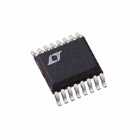
LTC3703EGN Linear Technology, LTC3703EGN Datasheet - Page 26

LTC3703EGN
Manufacturer Part Number
LTC3703EGN
Description
IC BUCK/BOOST SYNC ADJ 5A 16SSOP
Manufacturer
Linear Technology
Type
Step-Down (Buck), Step-Up (Boost)r
Datasheet
1.LTC3703EGNPBF.pdf
(32 pages)
Specifications of LTC3703EGN
Internal Switch(s)
No
Synchronous Rectifier
Yes
Number Of Outputs
1
Voltage - Output
0.8 ~ 93 V
Current - Output
5A
Frequency - Switching
100kHz ~ 600kHz
Voltage - Input
9.3 ~ 100 V
Operating Temperature
-40°C ~ 85°C
Mounting Type
Surface Mount
Package / Case
16-SSOP
Lead Free Status / RoHS Status
Contains lead / RoHS non-compliant
Power - Output
-
Available stocks
Company
Part Number
Manufacturer
Quantity
Price
Company:
Part Number:
LTC3703EGN
Manufacturer:
LINEAR
Quantity:
4
Part Number:
LTC3703EGN
Manufacturer:
LTNEAR
Quantity:
20 000
Company:
Part Number:
LTC3703EGN#PBF
Manufacturer:
LT
Quantity:
3 291
Part Number:
LTC3703EGN#PBF
Manufacturer:
LINEAR/凌特
Quantity:
20 000
Company:
Part Number:
LTC3703EGN#TRPBF
Manufacturer:
LT
Quantity:
3 291
Part Number:
LTC3703EGN#TRPBF
Manufacturer:
LTNEAR
Quantity:
20 000
Company:
Part Number:
LTC3703EGN-5
Manufacturer:
LT
Quantity:
10 000
Part Number:
LTC3703EGN-5
Manufacturer:
LINEAR/凌特
Quantity:
20 000
Company:
Part Number:
LTC3703EGN-5#PBF
Manufacturer:
LT
Quantity:
320
Part Number:
LTC3703EGN-5#PBF
Manufacturer:
LINEAR/凌特
Quantity:
20 000
APPLICATIONS INFORMATION
LTC3703
1. V
2. DRV
3. I
4. Transition losses apply only to the topside MOSFET in
Other losses including C
losses, Schottky conduction losses during dead time, and
inductor core losses generally account for less than 2%
total additional loss.
26
current given in the Electrical Characteristics table which
powers the internal control circuitry of the LTC3703.
Total supply current is typically about 2.5mA and usu-
ally results in a small (<1%) loss which is proportional
to V
results from switching the gate capacitance of the power
MOSFETs. Each time a MOSFET gate is switched on
and then off, a packet of gate charge Q
DRV
of the DRV
f(Q
the gate charges of the top and bottom MOSFETs.
MOSFETs, the inductor and input and output capacitor
ESR. In continuous mode, the average output current
fl ows through L but is “chopped” between the topside
MOSFET and the synchronous MOSFET. If the two
MOSFETs have approximately the same R
the resistance of one MOSFET can simply be summed
with the DCR resistance of L to obtain I
example, if each R
total resistance is 50mΩ. This results in losses ranging
from 1% to 5% as the output current increases from
1A to 5A for a 5V output.
buck mode and they become signifi cant when operat-
ing at higher input voltages (typically 20V or greater).
Transition losses can be estimated from the second
term of the P
Selection section.
The transition losses can become very signifi cant at
the high end of the LTC3703 operating voltage range.
To improve effi ciency, one may consider lowering the
frequency and/or using MOSFETs with lower C
the expense of higher R
2
CC
R losses are predicted from the DC resistances of
G(TOP)
CC
supply current. The V
CC
CC
.
current is MOSFET driver current. This current
to ground. The resulting dQ/dt is a current out
+ Q
CC
MAIN
G(BOT)
supply. In continuous mode, I
equation found in the Power MOSFET
DS(ON)
), where Q
IN
DS(ON)
= 25mΩ and R
CC
and C
current is the DC supply
.
G(TOP)
OUT
and Q
ESR dissipative
L
G
2
= 25mΩ, then
R losses. For
moves from
DS(ON)
G(BOT)
DRVCC
RSS
, then
are
at
=
Transient Response
Due to the high gain error amplifi er and line feedforward
compensation of the LTC3703, the output accuracy due to
DC variations in input voltage and output load current will
be almost negligible. For the few cycles following a load
transient, however, the output deviation may be larger while
the feedback loop is responding. Consider a typical 48V
input to 5V output application circuit, subjected to a 1A
to 5A load transient. Initially, the loop is in regulation and
the DC current in the output capacitor is zero. Suddenly,
an extra 4A (= 5A – 1A) fl ows out of the output capacitor
while the inductor is still supplying only 1A. This sudden
change will generate a (4A) • (R
output; with a typical 0.015Ω output capacitor ESR, this
is a 60mV step at the output.
The feedback loop will respond and will move at the
bandwidth allowed by the external compensation network
towards a new duty cycle. If the unity-gain crossover
frequency is set to 50kHz, the COMP pin will get to 60%
of the way to 90% duty cycle in 3μs. Now the inductor is
seeing 43V across itself for a large portion of the cycle
and its current will increase from 1A at a rate set by
di/dt = V/L. If the inductor value is 10μH, the peak di/dt
will be 43V/10μH or 4.3A/μs. Sometime in the next few
microseconds after the switch cycle begins, the inductor
current will have risen to the 5A level of the load current
and the output voltage will stop dropping. At this point,
the inductor current will rise somewhat above the level
of the output current to replenish the charge lost from
the output capacitor during the load transient. With a
properly compensated loop, the entire recovery time will
be inside of 10μs.
Most loads care only about the maximum deviation from
ideal, which occurs somewhere in the fi rst two cycles after
the load step hits. During this time, the output capacitor
does all the work until the inductor and control loop regain
control. The initial drop (or rise if the load steps down) is
entirely controlled by the ESR of the capacitor and amounts
to most of the total voltage drop. To minimize this drop,
choose a low ESR capacitor and/or parallel multiple capaci-
tors at the output. The capacitance value accounts for the
rest of the voltage drop until the inductor current rises.
ESR
) voltage step at the
3703fb


