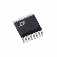
LTC3703EGN Linear Technology, LTC3703EGN Datasheet - Page 21

LTC3703EGN
Manufacturer Part Number
LTC3703EGN
Description
IC BUCK/BOOST SYNC ADJ 5A 16SSOP
Manufacturer
Linear Technology
Type
Step-Down (Buck), Step-Up (Boost)r
Datasheet
1.LTC3703EGNPBF.pdf
(32 pages)
Specifications of LTC3703EGN
Internal Switch(s)
No
Synchronous Rectifier
Yes
Number Of Outputs
1
Voltage - Output
0.8 ~ 93 V
Current - Output
5A
Frequency - Switching
100kHz ~ 600kHz
Voltage - Input
9.3 ~ 100 V
Operating Temperature
-40°C ~ 85°C
Mounting Type
Surface Mount
Package / Case
16-SSOP
Lead Free Status / RoHS Status
Contains lead / RoHS non-compliant
Power - Output
-
Available stocks
Company
Part Number
Manufacturer
Quantity
Price
Company:
Part Number:
LTC3703EGN
Manufacturer:
LINEAR
Quantity:
4
Part Number:
LTC3703EGN
Manufacturer:
LTNEAR
Quantity:
20 000
Company:
Part Number:
LTC3703EGN#PBF
Manufacturer:
LT
Quantity:
3 291
Part Number:
LTC3703EGN#PBF
Manufacturer:
LINEAR/凌特
Quantity:
20 000
Company:
Part Number:
LTC3703EGN#TRPBF
Manufacturer:
LT
Quantity:
3 291
Part Number:
LTC3703EGN#TRPBF
Manufacturer:
LTNEAR
Quantity:
20 000
Company:
Part Number:
LTC3703EGN-5
Manufacturer:
LT
Quantity:
10 000
Part Number:
LTC3703EGN-5
Manufacturer:
LINEAR/凌特
Quantity:
20 000
Company:
Part Number:
LTC3703EGN-5#PBF
Manufacturer:
LT
Quantity:
320
Part Number:
LTC3703EGN-5#PBF
Manufacturer:
LINEAR/凌特
Quantity:
20 000
APPLICATIONS INFORMATION
Finally, choose a convenient resistor value for R1 (10k is
usually a good value). Now calculate the remaining values:
Boost Converter Design
The following sections discuss the use of the LTC3703 as
a step-up (boost) converter. In boost mode, the LTC3703
can step-up output voltages as high as 80V. These sections
discuss only the design steps specifi c to a boost converter.
(K is a constant used in the calculations)
f = chosen crossover frequency
G = 10
absolute gain)
TYPE 2 Loop:
TYPE 3 Loop:
K
C
C
R
R
K
C
C
R
R
C
R
1
1
2
2
B
2
2
3
3
B
=
=
=
=
=
=
=
=
=
=
=
=
tan
tan
C K
C K
(GAIN/20)
2
2
K
2
2
2
V
V
2
2
R
π
π • •
π
π
π
OUT
OUT
2
⎛
⎝ ⎜
−
V
V
(
( (
1
f K R
• • • •
REF
⎛
⎝ ⎜
• • •
REF
BOOST
• •
1
K
f G K R
f G R
2
f C
f C
BOOST
K
−
1
−
1
−
− −
2
( )
1
( ) )
1
R
•
R
V
V
)
4
1
1
1
(this converts GAIN in dB to G in
REF
REF
)
1
1
3
+
1
+
45
1
45
°
⎞
⎠ ⎟
°
⎞
⎠ ⎟
For the design steps common to both a buck and a boost,
see the applicable section in the buck mode section. An
example of a boost converter circuit is shown in the Typi-
cal Applications section. To operate the LTC3703 in boost
mode, the INV pin should be tied to the V
a voltage above 2V). Note that in boost mode, pulse-skip
operation and the line feedforward compensation are
disabled.
For a boost converter, the duty cycle of the main switch
is:
For high V
by the LTC3703’s maximum duty cycle which is typically
93%. The maximum output voltage is therefore:
Boost Converter: Inductor Selection
In a boost converter, the average inductor current equals
the average input current. Thus, the maximum average
inductor current can be calculated from:
Similar to a buck converter, choose the ripple current to
be 20% to 40% of I
then determines the inductor value as follows:
The minimum required saturation current for the induc-
tor is:
Boost Converter: Power MOSFET Selection
For information about choosing power MOSFETs for a
boost converter, see the Power MOSFET Selection sec-
tion for the buck converter, since MOSFET selection is
I
I
D
L
V
L(SAT)
L MAX
OUT MAX
(
=
=
V
V
Δ
(
IN MIN
OUT
)
I
> I
V
(
L
OUT
=
OUT
•
L(MAX)
–
)
1
I
f
=
O MAX
−
)
to V
V
(
•
D
IN
1
V
D
MAX
–
IN MIN
MAX
IN
D
+ ΔI
(
)
L(MAX)
MAX
ratios, the maximum V
=
L
)
I
/2
O MAX
≅
(
. The ripple current amplitude
14
V
)
IN MIN
•
(
V
IN MIN
V
(
)
O
LTC3703
)
CC
OUT
voltage (or
is limited
21
3703fb


