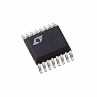
LTC3703EGN Linear Technology, LTC3703EGN Datasheet - Page 28

LTC3703EGN
Manufacturer Part Number
LTC3703EGN
Description
IC BUCK/BOOST SYNC ADJ 5A 16SSOP
Manufacturer
Linear Technology
Type
Step-Down (Buck), Step-Up (Boost)r
Datasheet
1.LTC3703EGNPBF.pdf
(32 pages)
Specifications of LTC3703EGN
Internal Switch(s)
No
Synchronous Rectifier
Yes
Number Of Outputs
1
Voltage - Output
0.8 ~ 93 V
Current - Output
5A
Frequency - Switching
100kHz ~ 600kHz
Voltage - Input
9.3 ~ 100 V
Operating Temperature
-40°C ~ 85°C
Mounting Type
Surface Mount
Package / Case
16-SSOP
Lead Free Status / RoHS Status
Contains lead / RoHS non-compliant
Power - Output
-
Available stocks
Company
Part Number
Manufacturer
Quantity
Price
Company:
Part Number:
LTC3703EGN
Manufacturer:
LINEAR
Quantity:
4
Part Number:
LTC3703EGN
Manufacturer:
LTNEAR
Quantity:
20 000
Company:
Part Number:
LTC3703EGN#PBF
Manufacturer:
LT
Quantity:
3 291
Part Number:
LTC3703EGN#PBF
Manufacturer:
LINEAR/凌特
Quantity:
20 000
Company:
Part Number:
LTC3703EGN#TRPBF
Manufacturer:
LT
Quantity:
3 291
Part Number:
LTC3703EGN#TRPBF
Manufacturer:
LTNEAR
Quantity:
20 000
Company:
Part Number:
LTC3703EGN-5
Manufacturer:
LT
Quantity:
10 000
Part Number:
LTC3703EGN-5
Manufacturer:
LINEAR/凌特
Quantity:
20 000
Company:
Part Number:
LTC3703EGN-5#PBF
Manufacturer:
LT
Quantity:
320
Part Number:
LTC3703EGN-5#PBF
Manufacturer:
LINEAR/凌特
Quantity:
20 000
APPLICATIONS INFORMATION
LTC3703
Next, choose the top and bottom MOSFET switch. Since
the drain of each MOSFET will see the full supply voltage
72V (max) plus any ringing, choose a 100V MOSFET to
provide a margin of safety. Si7456DP has a 100V BV
R
– 10nC)/50V = 180pF , V
The power dissipation can be estimated at maximum input
voltage, assuming a junction temperature of 100°C (30°C
above an ambient of 70°C):
And double check the assumed T
Since the synchronous MOSFET will be conducting over
twice as long each period (almost 100% of the period
in short circuit) as the top MOSFET, use two Si7456DP
MOSFETs on the bottom:
Next, set the current limit resistor. Since I
limit should be set such that the minimum current limit is
>10A. Minimum current limit occurs at maximum R
Using the above calculation for bottom MOSFET T
R
Therefore, I
= 0.215V. The R
0.215V/12μA = 18k.
C
(I
OS-CON capacitors (18mΩ each) are used to minimize
28
P
MAIN
IN
DS(ON)
DS(ON)
MAX
T
T
P
J
J
is chosen for an RMS current rating of about 5A
SYNC
/2) at 85°C. For the output capacitor, two low ESR
= 70°C + (1.64W)(20°C/W) = 103°C
= 70°C + (1.74W)(20°C/W) = 105°C
=
+
=
( ) )
0 70
12
72
= (25mΩ/2) [1 + 0.009 (105-25)] = 21.5mΩ.
= 25mΩ (max), δ = 0.009/°C, C
72
.
=
( )
MAX
⎛
⎝ ⎜
⎛
⎝ ⎜
10
2
W
0
⎛
⎝ ⎜
72 12
. .
10
025
+
pin voltage should be set to (10A)(0.0215)
2
2
2
72
−
SET
[
0 94
1 0 009 100 25 0 025
⎞
⎠ ⎟
.
+
( )(
⎞
⎠ ⎟
2 180
resistor can now be chosen to be
⎞
⎠ ⎟
=
W
.
( )
1 74
10
GS(MILLER)
=
.
1 64
(
pF
2
.
W
[
1 0 009 100 25
) •
+
W
–
⎛
⎝ ⎜
J
10 4 7
.
in the MOSFET:
= 4.7V, θ
) ( .
– .
]
1
(
MILLER
MAX
+
JA
–
4 7
)
1
.
= 10A, the
= 20°C/W.
J
⎞
⎠ ⎟
, the max
) •
= (19nC
(
]
DS(ON)
2
5 5 0
DSS
k
)
,
.
output voltage changes due to inductor current ripple and
load steps. The ripple voltage will be:
However, a 0A to 10A load step will cause an output volt-
age change of up to:
PC Board Layout Checklist
When laying out the printed circuit board, the following
checklist should be used to ensure proper operation of the
LTC3703. These items are also illustrated graphically in the
layout diagram of Figure 18. For layout of a boost mode
converter, layout is similar with V
Check the following in your layout:
1. Keep the signal and power grounds separate. The signal
2. The high di/dt loop formed by the top N-channel MOSFET,
3. Connect the drain of the top side MOSFET directly to the
4. Place the ceramic C
ΔV
= 36mV
ΔV
ground consists of the LTC3703 GND pin, the ground
return of C
ground consists of the Schottky diode anode, the source
of the bottom side MOSFET, and the (–) terminal of the
input capacitor and DRV
and power grounds together at the (–) terminal of the
output capacitor. Also, try to connect the (–) terminal
of the output capacitor as close as possible to the (–)
terminals of the input and DRV
from the Schottky loop described in (2).
the bottom MOSFET and the C
short leads and PC trace lengths to minimize high
frequency noise and voltage stress from inductive
ringing.
(+) plate of C
side MOSFET directly to the (–) terminal of C
capacitor provides the AC current to the MOSFETs.
diately next to the IC, between DRV
capacitor carries the MOSFET drivers’ current peaks.
Likewise the C
between BOOST and SW.
OUT(RIPPLE)
OUT(STEP)
VCC
= ΔI
IN
, and the (–) terminal of V
B
= ΔI
, and connect the source of the bottom
capacitor should also be next to the IC
LOAD(ESR)
L(MAX)
DRVCC
CC
(ESR) = (4A)(0.018Ω/2)
decoupling capacitor imme-
capacitor. Connect the signal
= (10A)(0.009Ω) = 90mV
IN
CC
IN
capacitor should have
and V
CC
capacitor and away
and BGRTN. This
OUT
OUT
. The power
swapped.
IN
. This
3703fb


