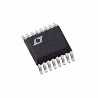
LTC3703EGN Linear Technology, LTC3703EGN Datasheet - Page 29

LTC3703EGN
Manufacturer Part Number
LTC3703EGN
Description
IC BUCK/BOOST SYNC ADJ 5A 16SSOP
Manufacturer
Linear Technology
Type
Step-Down (Buck), Step-Up (Boost)r
Datasheet
1.LTC3703EGNPBF.pdf
(32 pages)
Specifications of LTC3703EGN
Internal Switch(s)
No
Synchronous Rectifier
Yes
Number Of Outputs
1
Voltage - Output
0.8 ~ 93 V
Current - Output
5A
Frequency - Switching
100kHz ~ 600kHz
Voltage - Input
9.3 ~ 100 V
Operating Temperature
-40°C ~ 85°C
Mounting Type
Surface Mount
Package / Case
16-SSOP
Lead Free Status / RoHS Status
Contains lead / RoHS non-compliant
Power - Output
-
Available stocks
Company
Part Number
Manufacturer
Quantity
Price
Company:
Part Number:
LTC3703EGN
Manufacturer:
LINEAR
Quantity:
4
Part Number:
LTC3703EGN
Manufacturer:
LTNEAR
Quantity:
20 000
Company:
Part Number:
LTC3703EGN#PBF
Manufacturer:
LT
Quantity:
3 291
Part Number:
LTC3703EGN#PBF
Manufacturer:
LINEAR/凌特
Quantity:
20 000
Company:
Part Number:
LTC3703EGN#TRPBF
Manufacturer:
LT
Quantity:
3 291
Part Number:
LTC3703EGN#TRPBF
Manufacturer:
LTNEAR
Quantity:
20 000
Company:
Part Number:
LTC3703EGN-5
Manufacturer:
LT
Quantity:
10 000
Part Number:
LTC3703EGN-5
Manufacturer:
LINEAR/凌特
Quantity:
20 000
Company:
Part Number:
LTC3703EGN-5#PBF
Manufacturer:
LT
Quantity:
320
Part Number:
LTC3703EGN-5#PBF
Manufacturer:
LINEAR/凌特
Quantity:
20 000
APPLICATIONS INFORMATION
5. Place the small-signal components away from high
6. A separate decoupling capacitor for the supply, V
frequency switching nodes (BOOST, SW, TG, and BG).
In the layout shown in Figure 20, all the small-signal
components have been placed on one side of the IC
and all of the power components have been placed on
the other. This also helps keep the signal ground and
power ground isolated.
is useful with an RC fi lter between the DRV
and V
Connect this capacitor close to the IC, between the
V
capacitor (signal ground) isolated from the ground side
of the DRV
CC
and GND pins and keep the ground side of the V
CC
pin to fi lter any noise injected by the drivers.
CC
capacitor (power ground).
C
R
C2
C2
C
C3
R1
R2
R
C1
C
C1
R
R
C
MAX
SET
SS
Figure 20. LTC3703 Buck Converter Suggested Layout
1
2
3
4
5
6
7
8
MODE/SYNC
f
COMP
FB
I
INV
RUN/SS
GND
SET
MAX
LTC3703
BOOST
BGRTN
DRV
CC
V CC
SW
V
TG
BG
CC
IN
supply
16
15
14
13
12
11
10
9
CC
CC
,
C
X5R
VCC
V
CC
7. For optimum load regulation and true remote sensing,
8. For applications with multiple switching power con-
C
X5R
the top of the output resistor divider should connect
independently to the top of the output capacitor (Kelvin
connection), staying away from any high dV/dt traces.
Place the divider resistors near the LTC3703 in order
to keep the high impedance FB node short.
verters connected to the same input supply, make
sure that the input fi lter capacitor for the LTC3703 is
not shared with other converters. AC input current
from another converter could cause substantial input
voltage ripple, and this could interfere with the opera-
tion of the LTC3703. A few inches of PC trace or wire
(L ≅ 100nH) between C
source V
interference problems.
R
DRVCC
F
D
C
M2
B
M1
B
IN
V
should be suffi cient to prevent input noise
IN
D1
+
C
IN
IN
L1
C
OUT
of the LTC3703 and the actual
+
3703 F18
V
LTC3703
OUT
+
–
29
3703fb


