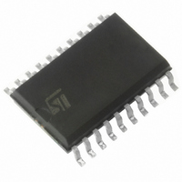
E-L6911C STMicroelectronics, E-L6911C Datasheet - Page 3

E-L6911C
Manufacturer Part Number
E-L6911C
Description
IC CTRLR 5BIT PROGR STPDN 20SOIC
Manufacturer
STMicroelectronics
Type
Step-Down (Buck)r
Datasheet
1.E-L6911C.pdf
(20 pages)
Specifications of E-L6911C
Internal Switch(s)
No
Synchronous Rectifier
Yes
Number Of Outputs
1
Voltage - Output
1.3 ~ 3.5 V
Current - Output
1.3A
Frequency - Switching
200kHz
Voltage - Input
5 ~ 12 V
Operating Temperature
-40°C ~ 150°C
Mounting Type
Surface Mount
Package / Case
20-SOIC (7.5mm Width)
Lead Free Status / RoHS Status
Lead free / RoHS Compliant
Power - Output
-
Lead Free Status / Rohs Status
Lead free / RoHS Compliant
Available stocks
Company
Part Number
Manufacturer
Quantity
Price
PIN FUNCTION
Num.
4 - 8
Pin
10
11
12
13
14
15
16
17
18
19
20
1
2
3
9
PGOOD This pin is an open collector output and is pulled low if the output voltage is not within the above
VID0 - 4
OCSET
SS/INH
PHASE
UGATE
LGATE
COMP
PGND
Name
VSEN
BOOT
GND
VCC
OVP
RT
FB
Connected to the output voltage is able to manage over-voltage conditions and the PGOOD
signal.
A resistor connected from this pin and the upper Mos Drain sets the current limit protection.
The internal 200 A current generator sinks a current from the drain through the external resistor.
The Over-Current threshold is due to the following equation:
The soft start time is programmed connecting an external capacitor from this pin and GND. The
internal current generator forces through the capacitor 10 A.
This pin can be used to disable the device forcing a voltage lower than 0.4V
Voltage Identification Code pins. These input are internally pulled-up and TTL compatible. They
are used to program the output voltage as specified in Table 1 and to set the overvoltage and
power good thresholds.
Connect to GND to program a ‘0’ while leave floating to program a ‘1’.
This pin is connected to the error amplifier output and is used to compensate the voltage control
feedback loop.
This pin is connected to the error amplifier inverting input and is used to compensate the voltage
control feedback loop.
All the internal references are referred to this pin. Connect it to the PCB signal ground.
specified thresholds.
If not used may be left floating.
This pin is connected to the source of the upper mosfet and provides the return path for the high
side driver. This pin monitors the drop across the upper mosfet for the current limit
High side gate driver output.
Bootstrap capacitor pin. Through this pin is supplied the high side driver and the upper mosfet.
Connect through a capacitor to the PHASE pin and through a diode to Vcc (cathode vs. boot).
Power ground pin. This pin has to be connected closely to the low side mosfet source in order to
reduce the noise injection into the device
This pin is the lower mosfet gate driver output
Device supply voltage. The operative nominal supply voltage ranges from 5 to 12V.
DO NOT CONNECT V
Over voltage protection. If the output voltage reaches the 17% above the programmed voltage
this pin is driven high and can be used to drive an external SCR that crowbar the supply voltage.
If not used, it may be left floating.
Oscillator switching frequency pin. Connecting an external resistor from this pin to GND, the
external frequency is increased according to the equation:
Connecting a resistor from this pin to Vcc (12V), the switching frequency is reduced according to
the equation:
If the pin is not connected, the switching frequency is 200KHz.
The voltage at this pin is fixed at 1.23V (typ). Forcing a 50 A current into this pin, the built in
oscillator stops to switch.
IN
TO A VOLTAGE GREATER THAN V
f
f
S
S
I
P
=
=
=
200kHz
200kHz
Description
I
--------------------------------------------- -
OCSE T
R
–
DS on
+
4.306 10
---------------------------- -
R
4.94 10
-------------------------
R
R
O CS ET
T
T
k
k
6
7
CC
.
L6911C
3/20


