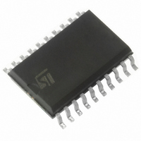
E-L6911C STMicroelectronics, E-L6911C Datasheet - Page 7

E-L6911C
Manufacturer Part Number
E-L6911C
Description
IC CTRLR 5BIT PROGR STPDN 20SOIC
Manufacturer
STMicroelectronics
Type
Step-Down (Buck)r
Datasheet
1.E-L6911C.pdf
(20 pages)
Specifications of E-L6911C
Internal Switch(s)
No
Synchronous Rectifier
Yes
Number Of Outputs
1
Voltage - Output
1.3 ~ 3.5 V
Current - Output
1.3A
Frequency - Switching
200kHz
Voltage - Input
5 ~ 12 V
Operating Temperature
-40°C ~ 150°C
Mounting Type
Surface Mount
Package / Case
20-SOIC (7.5mm Width)
Lead Free Status / RoHS Status
Lead free / RoHS Compliant
Power - Output
-
Lead Free Status / Rohs Status
Lead free / RoHS Compliant
Available stocks
Company
Part Number
Manufacturer
Quantity
Price
charge the output capacitor. As V
MOS begins to switch and the output voltage starts to increase.
The V
creases, as shown in figure 2. In this phase the system works in open loop. When V
clamp on the output of the error amplifier is released. In any case another clamp on the input of the error ampli-
fier remains active, allowing to V
In this second phase the system works in closed loop with a growing reference. As the output voltage reaches
the desired value V
increases until a maximum value of about 4V.
The Soft-Start will not take place, and the relative pin is internally shorted to GND, if both VCC and OCSET pins
are not above their own turn-on thresholds. During normal operation, if any under-voltage is detected on one of
the two supplies, the SS pin is internally shorted to GND and so the SS capacitor is rapidly discharged.
The device goes in INHIBIT state forcing SS pin below 0.4V. In this condition both external MOSFETS are kept
off.
Figure 2. Soft Start
Driver Section
The driver capability on the high and low side drivers allows using different types of power MOS (also multiple
MOS to reduce the R
The low-side mos driver is supplied directly by Vcc while the high-side driver is supplied by the BOOT pin.
Adaptative dead time control is implemented to prevent cross-conduction and allow to use several kinds of mos-
fets. The upper mos turn-on is avoided if the lower gate is over about 200mV while the lower mos turn-on is
avoided if the PHASE pin is over about 500mV. The upper mos is in any case turned-on after 200nS from the
low side turn-off.
The peak current is shown for both the upper (fig. 3) and the lower (fig. 4) driver at 5V and 12V. A 4nF capacitive
load has been used in these measurements.
For the lower driver, the source peak current is 1.1A @ Vcc=12V and 500mA @ Vcc=5V, and the sink peak
current is 1.3A @ Vcc=12V and 500mA @ Vcc=5V.
Similarly, for the upper driver, the source peak current is 1.3A @ Vboot-Vphase=12V and 600mA @ Vboot-
Vphase =5V, and the sink peak current is 1.3A @ Vboot-Vphase =12V and 550mA @ Vboot-Vphase = 5V.
SS
LGATE
growing voltage initially clamps the output of the error amplifier, and consequently V
Vout
V cc
V ss
Vin
to G ND
PROG
Timing Diagram
DSON
, also the clamp on the error amplifier input is removed, and the soft start finishes. Vss
), maintaining fast switching transition.
V cc Turn-on threshold
V in Turn-on threshold
1V
OUT
0.5V
SS
reaches 1V (i.e. the oscillator triangular wave inferior limit) also the upper
to grow with a lower slope (i.e. the slope of the V
Aquisition: CH1 = PHASE; CH2 = V
CH3 = PGOOD; CH4 = V
SS
SS
is equal to V
SS
voltage, see figure 2).
OUT
OUT
linearly in-
L6911C
COMP
;
7/20
the


