HCNR201-300E Avago Technologies US Inc., HCNR201-300E Datasheet - Page 8
HCNR201-300E
Manufacturer Part Number
HCNR201-300E
Description
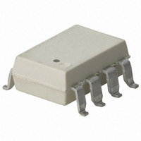
OPTOCOUPLER ANLG DC-1MHZ GW 8SMD
Manufacturer
Avago Technologies US Inc.
Specifications of HCNR201-300E
Output Type
Linear Photovoltaic
Input Type
DC
Package / Case
8-SMD Gull Wing
Number Of Channels
1
Voltage - Isolation
5000Vrms
Current Transfer Ratio (min)
0.36% @ 10mA
Current Transfer Ratio (max)
0.72% @ 10mA
Current - Dc Forward (if)
25mA
Mounting Type
Surface Mount, Gull Wing
Current Transfer Ratio
0.36 % to 0.72 %
Forward Current
1 mA to 20 mA
Isolation Voltage
5000 Vrms
Minimum Forward Diode Voltage
1.2 V
Output Device
Photodiode
Configuration
1 Channel
Maximum Forward Diode Voltage
1.95 V
Maximum Reverse Diode Voltage
2.5 V
Maximum Input Diode Current
25 mA
Maximum Power Dissipation
60 mW
Maximum Operating Temperature
+ 100 C
Minimum Operating Temperature
- 55 C
No. Of Channels
1
Optocoupler Output Type
Photodiode
Input Current
20mA
Output Voltage
15V
Opto Case Style
SMD
No. Of Pins
8
Forward Voltage
1.6V
Rohs Compliant
Yes
Forward Current If
25mA
Lead Free Status / RoHS Status
Lead free / RoHS Compliant
Voltage - Output
-
Current - Output / Channel
-
Vce Saturation (max)
-
Lead Free Status / Rohs Status
Lead free / RoHS Compliant
Other names
516-1609-5
Available stocks
Company
Part Number
Manufacturer
Quantity
Price
Company:

Part Number:
HCNR201-300E
Manufacturer:
AVAGO
Quantity:
30 000


Electrical Specifications
T
Parameter
Transfer Gain
Temperature
Coefficient of
Transfer Gain
DC NonLinearity
(Best Fit)
DC Nonlinearity
(Ends Fit)
Input Photo‑
diode Current
Transfer Ratio
(I
Temperature
Coefficient
of K
Photodiode
Leakage Current
Photodiode
Reverse Break‑
down Voltage
Photodiode
Capacitance
LED Forward
Voltage
LED Reverse
Breakdown
Voltage
Temperature
Coefficient of
Forward Voltage
LED Junction
Capacitance
8
A
= 25°C unless otherwise specified.
PD1
/I
1
F
)
∆K
∆K
∆V
Symbol
BV
NL
NL
C
C
BV
F
K
3
K
V
1
I
LK
/∆T
LED
/∆T
/∆T
PD
RPD
3
1
F
BF
EF
R
A
A
A
HCNR200
HCNR201
HCNR201
HCNR200
HCNR201
HCNR201
HCNR200
HCNR201
Device
Min.
0.85
0.95
0.93
0.25
0.36
1.3
1.2
2.5
30
0.016
1.00
1.00
1.00
0.01
0.01
0.01
0.50
0.48
Typ.
‑65
‑0.3
150
‑1.7
0.5
1.6
1.6
22
80
9
Max.
1.15
1.05
1.07
0.25
0.05
0.07
0.75
0.72
1.85
1.95
25
ppm/°C
mV/°C
Units
%/°C
nA
pF
pF
%
%
%
V
V
V
5 nA < I
0 V < V
5 nA < I
0 V < V
‑40°C < T
5 nA < I
0 V < V
‑40°C < T
5 nA < I
0 V < V
5 nA < I
0 V < V
5 nA < I
0 V < V
‑40°C < T
5 nA < I
0 V < V
5 nA < I
0 V < V
I
0 V < V
‑40°C < T
I
0 V < V
I
0 V < V
I
V
I
I
‑40°C < T
I
I
f = 1 MHz,
V
F
F
F
R
F
F
F
F
F
PD
= 10 mA,
= 10 mA
= 0 mA,
= 100 µA
= 10 mA
= 10 mA,
= 100 µA
= 10 mA
= 0 V
Test Conditions
= 0 V
PD
PD
PD
PD1
PD
PD
PD
PD
PD
PD1
PD
PD
PD
PD
PD
PD
PD
PD
PD
< 15 V
< 15 V
< 15 V
< 15 V
< 15 V
< 15 V
< 15 V
< 15 V
< 15 V
A
A
A
A
A
< 15 V
< 15 V
< 50 µA,
< 50 µA,
< 50 µA,
< 50 µA,
< 50 µA,
< 50 µA,
< 50 µA,
< 50 µA,
< 85°C,
< 85°C,
< 85°C,
< 85°C,
< 85°C
Fig.
4,5,
2,3
2,3
10
9,
6
7
7
8
Note
1
1
1
2
2
2
3
Related parts for HCNR201-300E
Image
Part Number
Description
Manufacturer
Datasheet
Request
R

Part Number:
Description:
OPTOCOUPLER, PHOTODIODE, 5000VRMS
Manufacturer:
Avago Technologies US Inc.
Datasheet:

Part Number:
Description:
OPTOCOUPLR ANLG HI-LIN 8DIP WIDE
Manufacturer:
Avago Technologies US Inc.
Datasheet:
Part Number:
Description:
OPTOCOUPLR ANLG HI-LIN 8DIP WIDE
Manufacturer:
Avago Technologies US Inc.
Datasheet:

Part Number:
Description:
Transistor/Diode Output Optocoupler
Manufacturer:
Avago Technologies US Inc.
Datasheet:

Part Number:
Description:
OPTOCOUPLER ANLG DC-1MHZ GW 8SMD
Manufacturer:
Avago Technologies US Inc.
Datasheet:

Part Number:
Description:
OPTOCOUPLER ANALOG VDE 8-SMD
Manufacturer:
Avago Technologies US Inc.
Datasheet:

Part Number:
Description:
OPTOCOUPLER ANALOG IEC 8-SMD
Manufacturer:
Avago Technologies US Inc.
Datasheet:
Part Number:
Description:
OPTOCOUPLER ANALOG VDE 8-DIP
Manufacturer:
Avago Technologies US Inc.
Datasheet:
Part Number:
Description:
OPTOCOUPLER ANALOG IEC 8-DIP
Manufacturer:
Avago Technologies US Inc.
Datasheet:
Part Number:
Description:
OPTOCOUPLER ANALOG VDE 8-SMD GW
Manufacturer:
Avago Technologies US Inc.
Datasheet:
Part Number:
Description:
OPTOCOUPLER, PHOTODIODE, 5000VRMS
Manufacturer:
Avago Technologies US Inc.
Datasheet:

Part Number:
Description:
OPTOCOUPLER GATE DRV 2A 16-SOIC
Manufacturer:
Avago Technologies US Inc.
Datasheet:
Part Number:
Description:
OPTOCOUPLER 2CH 2.5A 16-SOIC
Manufacturer:
Avago Technologies US Inc.
Datasheet:

Part Number:
Description:
OPTOCOUPLER GATE DRV 0.4A 16SOIC
Manufacturer:
Avago Technologies US Inc.
Datasheet:

Part Number:
Description:
OPTOCOUPLER 2.0A 250KHZ 8-DIP
Manufacturer:
Avago Technologies US Inc.
Datasheet: