MT9HTF6472AY-667D4 Micron Technology Inc, MT9HTF6472AY-667D4 Datasheet - Page 27

MT9HTF6472AY-667D4
Manufacturer Part Number
MT9HTF6472AY-667D4
Description
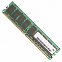
MODULE DDR2 512MB 240-DIMM
Manufacturer
Micron Technology Inc
Datasheet
1.MT9HTF12872AY-40ED1.pdf
(44 pages)
Specifications of MT9HTF6472AY-667D4
Memory Type
DDR2 SDRAM
Memory Size
512MB
Package / Case
240-DIMM
Lead Free Status / RoHS Status
Lead free / RoHS Compliant
Speed
-
Other names
557-1303
MT9HTF6472AY-667D4
MT9HTF6472AY-667D4
I
Table 13:
Table 14:
Capacitance
pdf: 09005aef80e6f860, source: 09005aef80e5b799
HTF9C32_64_128x72AG_2.fm - Rev. C 6/05 EN
Speed Grade
Speed Grade
-40E
-53E
-667
-40E
-53E
-667
DD
7 Conditions
I
All bank interleave READ operation
I
All bank interleave READ operation
DD
DD
A0 RA0 A1 RA1 A2 RA2 A3 RA3 A4 RA4 A5 RA5 A6 RA6 A7 RA7
A0 RA0 A1 RA1 A2 RA2 A3 RA3 D D A4 RA4 A5 RA5 A6 RA6 A7 RA7 D D
A0 RA0 D A1 RA1 D A2 RA2 D A3 RA3 D D A4 RA4 D A5 RA5 D A6 RA6 D A7 RA7 D D
A0 RA0 A1 RA1 A2 RA2 A3 RA3 D D D
A0 RA0 D A1 RA1 D A2 RA2 D A3 RA3 D D D D D
A0 RA0 D D A1 RA1 D D A2 RA2 D D A3 RA3 D D D D D D
7 Timing Patterns – 256MB and 512MB
7 Timing Patterns – 1GB
Table 13, I
– 1GB, specify detailed timing requirements for I
parameter changes are made to the specification.
Legend: A = active; RA = read auto precharge; D = deselect. All banks are being inter-
leaved at minimum
address bus inputs are STABLE during DESELECTs. I
At DDR2 data rates, Micron encourages designers to simulate the performance of the
module to achieve optimum values. When inductance and delay parameters associated
with trace lengths are used in simulations, they are significantly more accurate and real-
istic than a gross estimation of module capacitance. Simulations can then render a con-
siderably more accurate result. JEDEC modules are now designed by using simulations
to close timing budgets.
256MB, 512MB, 1GB (x72, SR, ECC) 240-Pin DDR2 SDRAM UDIMM
DD
7 Timing Patterns – 256MB and 512MB, and Table 14, I
t
RC (I
DD
Idd7 Timing Patterns
Idd7 Timing Patterns
) without violating
27
Micron Technology, Inc., reserves the right to change products or specifications without notice.
I
DD
t
RRD (I
DD
Specifications and Conditions
7. Changes will be required if timing
OUT
DD
©2003, 2004, 2005 Micron Technology, Inc. All rights reserved.
= 0mA.
) using a BL = 4. Control and
DD
7 Timing Patterns


