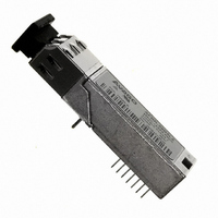
AFBR-59R5LZ Avago Technologies US Inc., AFBR-59R5LZ Datasheet - Page 8
AFBR-59R5LZ
Manufacturer Part Number
AFBR-59R5LZ
Description
TXRX OPT SFF 4/2/1GBD 2X7
Manufacturer
Avago Technologies US Inc.
Datasheet
1.AFBR-59R5LZ.pdf
(20 pages)
Specifications of AFBR-59R5LZ
Data Rate
4.25GBd
Wavelength
850nm
Voltage - Supply
3.6V
Connector Type
LC
Mounting Type
Through Hole
Function
Digital Diagnostic SFP, supports high-speed serial links over multimode optical fiber.
Product
Transceiver
Maximum Rise Time
0.09 ns/0.15 ns
Maximum Fall Time
0.09 ns/0.15 ns
Pulse Width Distortion
0.06 ns (Max)/0.062 ns (Max)
Operating Supply Voltage
2.97 V to 3.63 V
Maximum Operating Temperature
+ 85 C
Minimum Operating Temperature
- 10 C
Package / Case
DIP With Connector
Lead Free Status / RoHS Status
Lead free / RoHS Compliant
Applications
-
Lead Free Status / Rohs Status
Lead free / RoHS Compliant
For Use With
Multimode Glass
Lead Free Status / RoHS Status
Lead free / RoHS Compliant, Lead free / RoHS Compliant
Other names
516-1995


Table 3. Absolute Maximum Ratings
Table 4. Recommended Operating Conditions
Table 5. Transceiver Electrical Characteristics
(T
Notes:
1. Absolute Maximum Ratings are those values beyond which damage to the device may occur if these limits are exceeded for other than a
2. Between Absolute Maximum Ratings and the Recommended Operating Conditions functional performance is not intended, device reliability
3. The module supply voltages, V
4. Maximum wave or flow soldering temperature should not be applied for more than 10 seconds.
5. Recommended Operating Conditions are those values for which functional performance and device reliability is implied.
6. Filter per SFF specification is required on host board to remove 10 Hz to 4 MHz content.
7. SCL and SDA are to be pulled up externally with a 4.7 k – 10 k: resistor on the host board to 3.3 V.
8
Parameter
Storage Temperature
Case Operating Temperature
Aqueous Wash Pressure
Maximum Wave or Flow Soldering Temperature
Relative Humidity, non condensing
Supply Voltage
Voltage to any pin
Low Speed Input Voltage
Parameter
Case Operating Temperature
Supply Voltage
Data Rate
Parameter
AC Electrical Characteristics
Power Supply Noise Rejection (Peak-to-Peak)
DC Electrical Characteristics
Module Supply Current
Power Dissipation
Low Speed Outputs:
Signal Detect [SD], SDA
Low Speed Inputs:
Transmitter Disable [TX_DIS], SCL, SDA
C
short period of time. See Reliability Data Sheet for specific reliability performance.
is not implied, and damage to the device may occur over an extended period of time.
= -10°C to +85C, V
CC
T, V
CC
R = 3.3 V ± 10%)
CC
T and V
CC
R must not differ by more than 0.5 V or damage to the device may occur.
Symbol
T
T
T
RH
V
V
Symbol
T
V
Symbol
PSNR
I
P
V
V
V
V
CC
S
C
F
C
DISS
CC
IN
CC
OH
OL
IH
IL
T, R
T, R
Minimum
-40
-40
5
-0.5
-0.5
-0.5
Minimum
-10
2.97
1.0625
Minimum
100
2.0
2.00
Maximum
+100
+100
110
+260
95
3.8
3.8
V
Maximum
+85
3.63
4.25
Maximum
210
765
V
0.8
V
0.8
CC
CC
CC
T, R + 0.3
+ 0.5
Unit
°C
V
Gb/s
Unit
°C
°C
psi
°C
%
V
V
V
Unit
mV
mA
mW
V
V
V
V
Notes
1, 2
1, 2
4
1
1, 2, 3
1
Notes
5, 6
6, 7
6
Notes
6
TX + RX
7
Related parts for AFBR-59R5LZ
Image
Part Number
Description
Manufacturer
Datasheet
Request
R

Part Number:
Description:
650nm FE Transceiver Eval Kit
Manufacturer:
Avago Technologies US Inc.
Datasheet:

Part Number:
Description:
TXRX OPT OC3 MTRJ SFF 2X5DIP
Manufacturer:
Avago Technologies US Inc.
Datasheet:

Part Number:
Description:
TXRX ETHERNET 125MBD MMF 2X5
Manufacturer:
Avago Technologies US Inc.
Datasheet:

Part Number:
Description:
TXRX OPT SFP DGTL 850NM IND
Manufacturer:
Avago Technologies US Inc.
Datasheet:

Part Number:
Description:
TXRX OPT SFP 4/2/1GBD 850NM
Manufacturer:
Avago Technologies US Inc.
Datasheet:

Part Number:
Description:
TXRX OPT XFP 10GB/S 850NM
Manufacturer:
Avago Technologies US Inc.
Datasheet:

Part Number:
Description:
TXRX OPT 1X9 100MBPS ST EXT TEMP
Manufacturer:
Avago Technologies US Inc.
Datasheet:

Part Number:
Description:
TXRX OPT 1X9 100MBPS SC EXT TEMP
Manufacturer:
Avago Technologies US Inc.
Datasheet:

Part Number:
Description:
TXRX OPT 1X9 100MBPS DUPLEX SC
Manufacturer:
Avago Technologies US Inc.
Datasheet:

Part Number:
Description:
TXRX OPT 1X9 100MBPS DUPLEX ST
Manufacturer:
Avago Technologies US Inc.
Datasheet:

Part Number:
Description:
OPTOCOUPLER GATE DRV 2A 16-SOIC
Manufacturer:
Avago Technologies US Inc.
Datasheet:
Part Number:
Description:
OPTOCOUPLER 2CH 2.5A 16-SOIC
Manufacturer:
Avago Technologies US Inc.
Datasheet:

Part Number:
Description:
OPTOCOUPLER GATE DRV 0.4A 16SOIC
Manufacturer:
Avago Technologies US Inc.
Datasheet:

Part Number:
Description:
OPTOCOUPLER 2.0A 250KHZ 8-DIP
Manufacturer:
Avago Technologies US Inc.
Datasheet:

Part Number:
Description:
OPTOCOUPLER 2.0A 250KHZ GW 8-SMD
Manufacturer:
Avago Technologies US Inc.
Datasheet: