AFBR-59R5LZ Avago Technologies US Inc., AFBR-59R5LZ Datasheet - Page 9
AFBR-59R5LZ
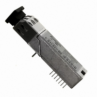
Manufacturer Part Number
AFBR-59R5LZ
Description
TXRX OPT SFF 4/2/1GBD 2X7
Manufacturer
Avago Technologies US Inc.
Datasheet
1.AFBR-59R5LZ.pdf
(20 pages)
Specifications of AFBR-59R5LZ
Data Rate
4.25GBd
Wavelength
850nm
Voltage - Supply
3.6V
Connector Type
LC
Mounting Type
Through Hole
Function
Digital Diagnostic SFP, supports high-speed serial links over multimode optical fiber.
Product
Transceiver
Maximum Rise Time
0.09 ns/0.15 ns
Maximum Fall Time
0.09 ns/0.15 ns
Pulse Width Distortion
0.06 ns (Max)/0.062 ns (Max)
Operating Supply Voltage
2.97 V to 3.63 V
Maximum Operating Temperature
+ 85 C
Minimum Operating Temperature
- 10 C
Package / Case
DIP With Connector
Lead Free Status / RoHS Status
Lead free / RoHS Compliant
Applications
-
Lead Free Status / Rohs Status
Lead free / RoHS Compliant
For Use With
Multimode Glass
Lead Free Status / RoHS Status
Lead free / RoHS Compliant, Lead free / RoHS Compliant
Other names
516-1995


Table 6. Transmitter and Receiver Electrical Characteristics
(T
Notes:
1. Internally ac coupled and terminated (100 Ohm differential).
2. Internally ac coupled but requires an external load termination (100 Ohm differential).
3. Contributed DJ is measured on an oscilloscope in average mode with 50% threshold and K28.5 pattern
4. Contributed TJ is the sum of contributed RJ and contributed DJ. Contributed RJ is calculated for 1x10
5. 20%-80% electrical rise & fall times measured with a 500 MHz signal utilizing a 1010 data pattern.
9
Parameter
High Speed Data Input:
Transmitter Differential Input Voltage (TD +/-)
High Speed Data Output:
Receiver Differential Output Voltage (RD +/-)
Receiver Contributed Total Jitter
(4.25 Gb/s)
Receiver Contributed Total Jitter
(2.125 Gb/s)
Receiver Contributed Total Jitter
(1.0625 Gb/s)
Receiver Electrical Output Rise & Fall Times
(20-80%)
C
(measured on a single rise or fall edge) from the oscilloscope by 14. Per FC-PI (Table 13 - MM jitter output, note 1), the actual contributed
RJ is allowed to increase above its limit if the actual contributed DJ decreases below its limits, as long as the component output DJ and TJ
remain within their specified FC-PI maximum limits with the worst case specified component jitter input.
= -10°C to +85°C, V
CC
T, V
CC
R = 3.3 V ± 10%)
Symbol
V
V
TJ
TJ
TJ
tr, tf
I
O
Minimum
400
600
50
Maximum
2400
1600
0.26
62
0.262
123
0.218
205
150
-12
BER by multiplying the RMS jitter
Unit
mV
mV
UI
ps
UI
ps
UI
ps
ps
Notes
1
2
4
4
4
5
Related parts for AFBR-59R5LZ
Image
Part Number
Description
Manufacturer
Datasheet
Request
R

Part Number:
Description:
650nm FE Transceiver Eval Kit
Manufacturer:
Avago Technologies US Inc.
Datasheet:

Part Number:
Description:
TXRX OPT OC3 MTRJ SFF 2X5DIP
Manufacturer:
Avago Technologies US Inc.
Datasheet:

Part Number:
Description:
TXRX ETHERNET 125MBD MMF 2X5
Manufacturer:
Avago Technologies US Inc.
Datasheet:

Part Number:
Description:
TXRX OPT SFP DGTL 850NM IND
Manufacturer:
Avago Technologies US Inc.
Datasheet:

Part Number:
Description:
TXRX OPT SFP 4/2/1GBD 850NM
Manufacturer:
Avago Technologies US Inc.
Datasheet:

Part Number:
Description:
TXRX OPT XFP 10GB/S 850NM
Manufacturer:
Avago Technologies US Inc.
Datasheet:

Part Number:
Description:
TXRX OPT 1X9 100MBPS ST EXT TEMP
Manufacturer:
Avago Technologies US Inc.
Datasheet:

Part Number:
Description:
TXRX OPT 1X9 100MBPS SC EXT TEMP
Manufacturer:
Avago Technologies US Inc.
Datasheet:

Part Number:
Description:
TXRX OPT 1X9 100MBPS DUPLEX SC
Manufacturer:
Avago Technologies US Inc.
Datasheet:

Part Number:
Description:
TXRX OPT 1X9 100MBPS DUPLEX ST
Manufacturer:
Avago Technologies US Inc.
Datasheet:

Part Number:
Description:
OPTOCOUPLER GATE DRV 2A 16-SOIC
Manufacturer:
Avago Technologies US Inc.
Datasheet:
Part Number:
Description:
OPTOCOUPLER 2CH 2.5A 16-SOIC
Manufacturer:
Avago Technologies US Inc.
Datasheet:

Part Number:
Description:
OPTOCOUPLER GATE DRV 0.4A 16SOIC
Manufacturer:
Avago Technologies US Inc.
Datasheet:

Part Number:
Description:
OPTOCOUPLER 2.0A 250KHZ 8-DIP
Manufacturer:
Avago Technologies US Inc.
Datasheet:

Part Number:
Description:
OPTOCOUPLER 2.0A 250KHZ GW 8-SMD
Manufacturer:
Avago Technologies US Inc.
Datasheet: