MA240017 Microchip Technology, MA240017 Datasheet - Page 127
MA240017
Manufacturer Part Number
MA240017
Description
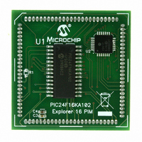
MODULE PLUG-IN PIC24F16KA102 PIM
Manufacturer
Microchip Technology
Series
PIC®r
Specifications of MA240017
Accessory Type
Plug-In Module (PIM) - PIC24F16KA102
Product
Microcontroller Modules
Data Bus Width
16 bit
Core Processor
PIC24F16KA102
Operating Supply Voltage
3 V to 3.6 V
Development Tools By Supplier
Integrated Development Environment, Assembler, ANSI C Compiler
Processor Series
PIC24F
Silicon Manufacturer
Microchip
Core Architecture
PIC
Core Sub-architecture
PIC24
Silicon Core Number
PIC24F
Silicon Family Name
PIC24FxxKAxx
Lead Free Status / RoHS Status
Lead free / RoHS Compliant
For Use With/related Products
Explorer 16 (DM240001 or DM240002)
For Use With
DM240001 - BOARD DEMO PIC24/DSPIC33/PIC32
Lead Free Status / Rohs Status
Lead free / RoHS Compliant
Available stocks
Company
Part Number
Manufacturer
Quantity
Price
Company:

Part Number:
MA240017
Manufacturer:
MICROCHIP
Quantity:
12 000


15.4
REGISTER 15-1:
© 2009 Microchip Technology Inc.
bit 15
bit 7
Legend:
R = Readable bit
-n = Value at POR
bit 15-14
bit 13
bit 12-5
bit 4
bit 3
bit 2-0
Note 1:
U-0
U-0
—
—
Output Compare Register
OCFA pin controls OC1 channel.
Unimplemented: Read as ‘0’
OCSIDL: Stop Output Compare 1 in Idle Mode Control bit
1 = Output Compare 1 will halt in CPU Idle mode
0 = Output Compare 1 will continue to operate in CPU Idle mode
Unimplemented: Read as ‘0’
OCFLT: PWM Fault Condition Status bit
1 = PWM Fault condition has occurred (cleared in HW only)
0 = No PWM Fault condition has occurred (this bit is only used when OCM<2:0> = 111)
OCTSEL: Output Compare 1 Timer Select bit
1 = Timer3 is the clock source for Output Compare 1
0 = Timer2 is the clock source for Output Compare 1
Refer to the device data sheet for specific time bases available to the output compare module.
OCM<2:0>: Output Compare 1 Mode Select bits
111 = PWM mode on OC1, Fault pin; OCF1 enabled
110 = PWM mode on OC1, Fault pin; OCF1 disabled
101 = Initialize OC1 pin low, generate continuous output pulses on OC1 pin
100 = Initialize OC1 pin low, generate single output pulse on OC1 pin
011 = Compare event toggles OC1 pin
010 = Initialize OC1 pin high, compare event forces OC1 pin low
001 = Initialize OC1 pin low, compare event forces OC1 pin high
000 = Output compare channel is disabled
U-0
U-0
—
—
OC1CON: OUTPUT COMPARE 1 CONTROL REGISTER
HC = Hardware Clearable bit
W = Writable bit
‘1’ = Bit is set
OCSIDL
R/W-0
U-0
—
R-0, HC
OCFLT
U-0
—
Preliminary
PIC24F16KA102 FAMILY
U = Unimplemented bit, read as ‘0’
‘0’ = Bit is cleared
OCTSEL
R/W-0
U-0
—
(1)
(1)
R/W-0
OCM2
U-0
—
x = Bit is unknown
OCM1
R/W-0
U-0
—
DS39927B-page 125
R/W-0
OCM0
U-0
—
bit 8
bit 0
Related parts for MA240017
Image
Part Number
Description
Manufacturer
Datasheet
Request
R

Part Number:
Description:
Manufacturer:
Microchip Technology Inc.
Datasheet:
Part Number:
Description:
Manufacturer:
Microchip Technology Inc.
Datasheet:
Part Number:
Description:
Manufacturer:
Microchip Technology Inc.
Datasheet:
Part Number:
Description:
Manufacturer:
Microchip Technology Inc.
Datasheet:
Part Number:
Description:
Manufacturer:
Microchip Technology Inc.
Datasheet:
Part Number:
Description:
Manufacturer:
Microchip Technology Inc.
Datasheet:
Part Number:
Description:
Manufacturer:
Microchip Technology Inc.
Datasheet:
Part Number:
Description:
Manufacturer:
Microchip Technology Inc.
Datasheet: