MA240017 Microchip Technology, MA240017 Datasheet - Page 47
MA240017
Manufacturer Part Number
MA240017
Description
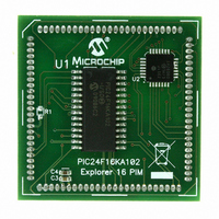
MODULE PLUG-IN PIC24F16KA102 PIM
Manufacturer
Microchip Technology
Series
PIC®r
Specifications of MA240017
Accessory Type
Plug-In Module (PIM) - PIC24F16KA102
Product
Microcontroller Modules
Data Bus Width
16 bit
Core Processor
PIC24F16KA102
Operating Supply Voltage
3 V to 3.6 V
Development Tools By Supplier
Integrated Development Environment, Assembler, ANSI C Compiler
Processor Series
PIC24F
Silicon Manufacturer
Microchip
Core Architecture
PIC
Core Sub-architecture
PIC24
Silicon Core Number
PIC24F
Silicon Family Name
PIC24FxxKAxx
Lead Free Status / RoHS Status
Lead free / RoHS Compliant
For Use With/related Products
Explorer 16 (DM240001 or DM240002)
For Use With
DM240001 - BOARD DEMO PIC24/DSPIC33/PIC32
Lead Free Status / Rohs Status
Lead free / RoHS Compliant
Available stocks
Company
Part Number
Manufacturer
Quantity
Price
Company:

Part Number:
MA240017
Manufacturer:
MICROCHIP
Quantity:
12 000


REGISTER 5-1:
© 2009 Microchip Technology Inc.
bit 15
bit 7
Legend:
-n = Value at POR
‘0’ = Bit is cleared
bit 15
bit 14
bit 13
bit 12
bit 11-7
bit 6
bit 5-0
Note 1:
R/SO-0, HC
WR
U-0
—
2:
3:
4:
All other combinations of NVMOP<5:0> are no operation.
Available in ICSP™ mode only. Refer to device programming specification.
The address in the Table Pointer decides which rows will be erased.
This bit is used only while accessing data EEPROM.
WR: Write Control bit
1 = Initiates a Flash memory program or erase operation. The operation is self-timed and the bit is
0 = Program or erase operation is complete and inactive
WREN: Write Enable bit
1 = Enable Flash program/erase operations
0 = Inhibit Flash program/erase operations
WRERR: Write Sequence Error Flag bit
1 = An improper program or erase sequence attempt or termination has occurred (bit is set automatically
0 = The program or erase operation completed normally
PGMONLY: Program Only Enable bit
Unimplemented: Read as ‘0’
ERASE: Erase/Program Enable bit
1 = Perform the erase operation specified by NVMOP<5:0> on the next WR command
0 = Perform the program operation specified by NVMOP<5:0> on the next WR command
NVMOP<5:0>: Programming Operation Command Byte bits
Erase Operations (when ERASE bit is ‘1’):
1010xx = Erase entire boot block (including code-protected boot block)
1001xx = Erase entire memory (including boot block, configuration block, general block)
011010 = Erase 4 rows of Flash memory
011001 = Erase 2 rows of Flash memory
011000 = Erase 1 row of Flash memory
0101xx = Erase entire configuration block (except code protection bits)
0100xx = Erase entire data EEPROM
0011xx = Erase entire general memory block programming operations
0001xx = Write 1 row of Flash memory (when ERASE bit is ‘0’)
ERASE
WREN
R/W-0
R/W-0
cleared by hardware once the operation is complete
on any set attempt of the WR bit)
NVMCON: FLASH MEMORY CONTROL REGISTER
x = Bit is unknown
SO = Settable Only bit
‘1’ = Bit is set
NVMOP5
WRERR
R/W-0
R/W-0
(1)
PGMONLY
NVMOP4
R/W-0
R/W-0
Preliminary
(4)
(4)
(1)
PIC24F16KA102 FAMILY
(4)
(3)
(3)
(3)
HC = Hardware Clearable bit
R = Readable bit
U = Unimplemented bit, read as ‘0’
NVMOP3
R/W-0
U-0
—
(1)
NVMOP2
(1)
R/W-0
U-0
(3)
—
(1)
(2)
W = Writable bit
NVMOP1
R/W-0
U-0
—
(1)
DS39927B-page 45
(2)
NVMOP0
R/W-0
U-0
—
bit 8
bit 0
(1)
Related parts for MA240017
Image
Part Number
Description
Manufacturer
Datasheet
Request
R

Part Number:
Description:
Manufacturer:
Microchip Technology Inc.
Datasheet:
Part Number:
Description:
Manufacturer:
Microchip Technology Inc.
Datasheet:
Part Number:
Description:
Manufacturer:
Microchip Technology Inc.
Datasheet:
Part Number:
Description:
Manufacturer:
Microchip Technology Inc.
Datasheet:
Part Number:
Description:
Manufacturer:
Microchip Technology Inc.
Datasheet:
Part Number:
Description:
Manufacturer:
Microchip Technology Inc.
Datasheet:
Part Number:
Description:
Manufacturer:
Microchip Technology Inc.
Datasheet:
Part Number:
Description:
Manufacturer:
Microchip Technology Inc.
Datasheet: