MA240017 Microchip Technology, MA240017 Datasheet - Page 55
MA240017
Manufacturer Part Number
MA240017
Description
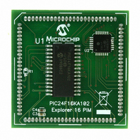
MODULE PLUG-IN PIC24F16KA102 PIM
Manufacturer
Microchip Technology
Series
PIC®r
Specifications of MA240017
Accessory Type
Plug-In Module (PIM) - PIC24F16KA102
Product
Microcontroller Modules
Data Bus Width
16 bit
Core Processor
PIC24F16KA102
Operating Supply Voltage
3 V to 3.6 V
Development Tools By Supplier
Integrated Development Environment, Assembler, ANSI C Compiler
Processor Series
PIC24F
Silicon Manufacturer
Microchip
Core Architecture
PIC
Core Sub-architecture
PIC24
Silicon Core Number
PIC24F
Silicon Family Name
PIC24FxxKAxx
Lead Free Status / RoHS Status
Lead free / RoHS Compliant
For Use With/related Products
Explorer 16 (DM240001 or DM240002)
For Use With
DM240001 - BOARD DEMO PIC24/DSPIC33/PIC32
Lead Free Status / Rohs Status
Lead free / RoHS Compliant
Available stocks
Company
Part Number
Manufacturer
Quantity
Price
Company:

Part Number:
MA240017
Manufacturer:
MICROCHIP
Quantity:
12 000


6.3
As with Flash program memory, the NVM Address
Registers, NVMADRU and NVMADR, form the 24-bit
Effective Address (EA) of the selected row or word for
data EEPROM operations. The NVMADRU register is
used to hold the upper 8 bits of the EA, while the
NVMADR register is used to hold the lower 16 bits of
the EA. These registers are not mapped into the
Special Function Register (SFR) space; instead, they
directly capture the EA<23:0> of the last table write
instruction that has been executed and selects the data
EEPROM row to erase. Figure 6-1 depicts the program
memory EA that is formed for programming and erase
operations.
FIGURE 6-1:
6.4
The EEPROM block is accessed using table read and
write operations similar to those used for program
memory. The TBLWTH and TBLRDH instructions are not
required for data EEPROM operations since the
memory is only 16 bits wide (data on the lower address
is valid only). The following programming operations
can be performed on the data EEPROM:
• Erase one, four or eight words
• Bulk erase the entire data EEPROM
• Write one word
• Read one word
© 2009 Microchip Technology Inc.
NVM Address Register
Data EEPROM Operations
DATA EEPROM ADDRESSING WITH TBLPAG AND NVM ADDRESS REGISTERS
0
NVMADRU
TBLPAG
7Fh
Preliminary
24-Bit PM Address
PIC24F16KA102 FAMILY
W Register EA
NVMADR
Like program memory operations, the Least Significant
bit (LSb) of NVMADR is restricted to even addresses.
This is because any given address in the data
EEPROM space consists of only the lower word of the
program memory width; the upper word, including the
uppermost “phantom byte”, are unavailable. This
means that the LSb of a data EEPROM address will
always be ‘0’.
Similarly, the Most Significant bit (MSb) of NVMADRU
is always ‘0’, since all addresses lie in the user program
space.
The library procedures are used in the code examples
detailed in the following sections. General descriptions
of each process are provided for users who are not
using the C30 compiler libraries.
xxxxh
Note 1: Unexpected results will be obtained
2: The C30 C compiler includes library
should the user attempt to read the
EEPROM while a programming or erase
operation is underway.
procedures to automatically perform the
table read and table write operations,
manage the Table Pointer and write
buffers, and unlock and initiate memory
write sequences. This eliminates the
need to create assembler macros or time
critical routines in C for each application.
0
DS39927B-page 53
Related parts for MA240017
Image
Part Number
Description
Manufacturer
Datasheet
Request
R

Part Number:
Description:
Manufacturer:
Microchip Technology Inc.
Datasheet:
Part Number:
Description:
Manufacturer:
Microchip Technology Inc.
Datasheet:
Part Number:
Description:
Manufacturer:
Microchip Technology Inc.
Datasheet:
Part Number:
Description:
Manufacturer:
Microchip Technology Inc.
Datasheet:
Part Number:
Description:
Manufacturer:
Microchip Technology Inc.
Datasheet:
Part Number:
Description:
Manufacturer:
Microchip Technology Inc.
Datasheet:
Part Number:
Description:
Manufacturer:
Microchip Technology Inc.
Datasheet:
Part Number:
Description:
Manufacturer:
Microchip Technology Inc.
Datasheet: