C8051T610DB32 Silicon Laboratories Inc, C8051T610DB32 Datasheet - Page 43
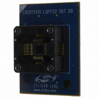
C8051T610DB32
Manufacturer Part Number
C8051T610DB32
Description
DAUGHT BOARD T610 32TQFP SOCKET
Manufacturer
Silicon Laboratories Inc
Datasheet
1.C8051T610DB32.pdf
(218 pages)
Specifications of C8051T610DB32
Module/board Type
Socket Module - TQFP
Processor To Be Evaluated
C8051T61x
Interface Type
USB
Lead Free Status / RoHS Status
Lead free / RoHS Compliant
For Use With/related Products
C8051T610DK
Lead Free Status / RoHS Status
Lead free / RoHS Compliant, Lead free / RoHS Compliant
Other names
336-1505


SFR Definition 8.1. ADC0CF: ADC0 Configuration
SFR Address = 0xBC
Name
Reset
Bit
7:3 AD0SC[4:0] ADC0 SAR Conversion Clock Period Bits.
Type
2
1
0
Bit
AMP0GN0 ADC Gain Control Bit.
AD0LJST
AD08BE
Name
7
1
SAR Conversion clock is derived from system clock by the following equation, where
AD0SC refers to the 5-bit value held in bits AD0SC4–0. SAR Conversion clock
requirements are given in the ADC specification table.
Note: If the Memory Power Controller is enabled (MPCE = '1'), AD0SC must be set to at least
ADC0 Left Justify Select.
0: Data in ADC0H:ADC0L registers are right-justified.
1: Data in ADC0H:ADC0L registers are left-justified.
Note: The AD0LJST bit is only valid for 10-bit mode (AD08BE = 0).
8-Bit Mode Enable.
0: ADC operates in 10-bit mode (normal).
1: ADC operates in 8-bit mode.
Note: When AD08BE is set to 1, the AD0LJST bit is ignored.
0: Gain = 0.5
1: Gain = 1
AD0SC
6
1
"00001" for proper ADC operation.
=
AD0SC[4:0]
SYSCLK
---------------------- - 1
CLK
R/W
5
1
SAR
–
Rev 1.0
4
1
C8051T610/1/2/3/4/5/6/7
Function
3
1
AD0LJST
R/W
2
0
AD08BE
R/W
1
0
AMP0GN0
R/W
0
1
43
Related parts for C8051T610DB32
Image
Part Number
Description
Manufacturer
Datasheet
Request
R

Part Number:
Description:
SMD/C°/SINGLE-ENDED OUTPUT SILICON OSCILLATOR
Manufacturer:
Silicon Laboratories Inc
Part Number:
Description:
Manufacturer:
Silicon Laboratories Inc
Datasheet:
Part Number:
Description:
N/A N/A/SI4010 AES KEYFOB DEMO WITH LCD RX
Manufacturer:
Silicon Laboratories Inc
Datasheet:
Part Number:
Description:
N/A N/A/SI4010 SIMPLIFIED KEY FOB DEMO WITH LED RX
Manufacturer:
Silicon Laboratories Inc
Datasheet:
Part Number:
Description:
N/A/-40 TO 85 OC/EZLINK MODULE; F930/4432 HIGH BAND (REV E/B1)
Manufacturer:
Silicon Laboratories Inc
Part Number:
Description:
EZLink Module; F930/4432 Low Band (rev e/B1)
Manufacturer:
Silicon Laboratories Inc
Part Number:
Description:
I°/4460 10 DBM RADIO TEST CARD 434 MHZ
Manufacturer:
Silicon Laboratories Inc
Part Number:
Description:
I°/4461 14 DBM RADIO TEST CARD 868 MHZ
Manufacturer:
Silicon Laboratories Inc
Part Number:
Description:
I°/4463 20 DBM RFSWITCH RADIO TEST CARD 460 MHZ
Manufacturer:
Silicon Laboratories Inc
Part Number:
Description:
I°/4463 20 DBM RADIO TEST CARD 868 MHZ
Manufacturer:
Silicon Laboratories Inc
Part Number:
Description:
I°/4463 27 DBM RADIO TEST CARD 868 MHZ
Manufacturer:
Silicon Laboratories Inc
Part Number:
Description:
I°/4463 SKYWORKS 30 DBM RADIO TEST CARD 915 MHZ
Manufacturer:
Silicon Laboratories Inc
Part Number:
Description:
N/A N/A/-40 TO 85 OC/4463 RFMD 30 DBM RADIO TEST CARD 915 MHZ
Manufacturer:
Silicon Laboratories Inc
Part Number:
Description:
I°/4463 20 DBM RADIO TEST CARD 169 MHZ
Manufacturer:
Silicon Laboratories Inc