ADNK-5033-FS27 Avago Technologies US Inc., ADNK-5033-FS27 Datasheet
ADNK-5033-FS27
Specifications of ADNK-5033-FS27


Related parts for ADNK-5033-FS27


ADNK-5033-FS27 Summary of contents
Page 1
... ADNK-5033-FS27 USB RF Wireless Optical Mouse Designer’ s Kit Design Guide Introduction This design guide describes how a small form power- effective optical mouse can be built using the Avago Technologies’ ADNS-5030 optical navigation sensor and Freescale Semiconductor’s MC68HC908QY4A and MC68HC908JB12 microcontroller. The document starts ...
Page 2
Mouse Buttons Mouse buttons are connected as standard switches. These switches are pulled up by the pull up resistors inside the microcontroller. When the user presses a button, the switch will be closed and the pin will be pulled LOW ...
Page 3
Wireless RF Technology A high data rate 27-MHz RF link is designed as the wireless communication media for this application. The RF frequency is determined by the crystal frequency used at the oscillator circuit stage. The transmission data rate is ...
Page 4
RF Receiver The RF receiver is implemented by using a single-chip solution (3361 compatible part) that includes: • A frequency downward conversion mixer • A local oscillator circuit • A baseband FSK quadrature demodulation unit The RF input signal from ...
Page 5
The communication between the sensor and the MC68HC908QY4A is through a serial peripheral interface (SPI) with clock input at the SCLK pin, the data interface at the MISO and MOSI pins. The receiver consists of: • The MC68HC908JB12 • A ...
Page 6
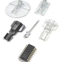
... To Disassemble the ADNK-5033-FS27 Unit The ADNK-5033-FS27 comprises of the plastic mouse casing, printed circuit board (PCB), lens, buttons, and USB cable (See Figure 5). Unscrewing the one screw located at the base of the unit can open the ADNK- 5033-FS27 unit ...
Page 7
... This includes PCB assembly diagrams like solder fixture in assembly and exploded view, as well as solder plate. See Appendix D for details. Reference Design Documentation – Gerber File The Gerber File presents detailed schematics used in ADNK-5033-FS27 in PCB layout form. See Appendix C for more details. contact Freescale Overall circuit A schematic of the overall circuit is shown in Appendix A of this document ...
Page 8
Firmware Implementation The MC68HC908QY4A mouse firmware is compiled under CodeWarrior environment from Freescale Semiconductor Inc. The firmware includes the following files: QY4 _OPTICAL_MOUSE.ASM Main program, includes power up entry point, constant and variables definition. QY4_INT.ASM Timer interrupt service routines RF ...
Page 9
Power Management Scheme Figure 8 shows the flow of the power management of the optical mouse. The ADNS-5030 has three internal power-saving modes. Each mode has a different motion detection period, affecting response time to mouse motion (Response Time). The ...
Page 10
RF Packet Structure All the mouse data is transmitted by RF front end with the FSK modulation. There are two types of RF packet: XY movement packet or Buttons status/Z movement packet. The Button status/Z movement packet will also be ...
Page 11
MC68HC908JB12 Receiver Firmware The MC68HC908JB12 receiver firmware is compiled under CASM08Z.EXE from P&E Microcomputer Inc. The firmware includes the following files: MOTSTART.asm Program entry point after power up or reset. Constant and Variable definition, I/O and timer initialization routines are ...
Page 12
MAIN NO DEVICE CONFIGURED? YES NO NEW RECEIVED MOUSE DATA IN BUFFER? YES CONVERT DATA TO MOUSE REPORT NEW ENDPOINT 1 REPORT? NO NEW ENDPOINT 2 REPORT? NO USB IDLE FOR 3 MS? NO Figure 9. Firmware Main Program Flow ...
Page 13
Figure 10. USB Interrupt Routine 13 ...
Page 14
Figure 11. USB Setup Routine Figure 12. OUT EPO Handler 14 ...
Page 15
Figure 13. IN EPO Handler 15 ...
Page 16
Figure 14. Timer Capture Routine for RF Receiver 16 ...
Page 17
USB Report Format The USB routines in the MC68HC908JB12 act as a composite device of keyboard and mouse. It implements two HID interfaces on endpoint 1 and endpoint 2. HID interface 0 (endpoint 1) implements a standard HID keyboard with ...
Page 18
Figure 15. Timing Parameters for Packet Detection Figure 16. Detection of Valid Wakeup Packets 18 ...
Page 19
Figure 17. Rejecting Packet-Like Noise to prevent false wakeup ID Updating Process The user must follow these steps to update the mouse ID: 1. Press and hold the “PTA0” button in the receiver 2. Press “CONNECT” button once in the ...
Page 20
Appendix A: Schematic Design of Overall Circuit + ...
Page 21
21 ...
Page 22
22 ...
Page 23
APPENDIX B : Bill Of Materials Table B1: Mouse Main board Part Description Quantity Value SMD RES (0603) 3 SMD RES (0603) 4 SMD RES (0603) 2 SMD RES (0603) 1 SMD CER CAP (0603) 3 SMD TANT CAP 1 ...
Page 24
Table B2: Bill Of Material for RF board Part Description Quantity Value SMD RES (0603) 4 SMD RES (0603) 2 SMD RES (0603) 2 SMD RES (0603) 1 SMD RES (0603) 1 SMD RES (0603) 1 SMD RES (0603) 1 ...
Page 25
Table B3: Bill Of Materials for Receiver Board Part Description Quantity Value SMD RES (0603) 1 SMD RES (0603) 1 SMD RES (0603) 2 SMD RES (0603) 2 SMD RES (0603) 1 SMD RES (0603) 1 SMD RES (0603) 2 ...
Page 26
APPENDIX C: PCB Layout Figure C1. Top Side PCB Layout (Mouse Main Board) Figure C2. Top Side Components (Mouse Main Board) 26 ...
Page 27
Figure C3. Bottom Side PCB Layout (Mouse Main Board) Figure C4. Bottom Side Components (Mouse Main Board) 27 ...
Page 28
Figure C5. Optical Mouse RF Board Top Layer Figure C6. Optical Mouse RF Board Top Overlay 28 ...
Page 29
Figure C7. Optical Mouse RF Board Bottom Layer Figure C8. Optical Mouse RF Board Bottom Overlay 29 ...
Page 30
Figure C9. USB Receiver Board Top Layer Figure C10. USB Receiver Board Top Overlay 30 ...
Page 31
Figure C11. USB Receiver Board Bottom Layer Figure C12. USB Receiver Board Bottom Overlay 31 ...
Page 32
... ADNS-5100-001 Trim Lens Plate ADNS-5200 LED Assembly Clip (Black) HLMP-ED80-XX000 639 ¾ (5 mm) Diameter LED ADNK-5033-FS27 Includes Documentation and Support Files for ADNK-5033-FS27 CD Documentation a. ADNS-5030 Data Sheet b. MC68HC908JB12 & MC68HC908QY4A Data Sheet c. ADNS-5100 Data Sheet d. ADNS-5200 Data Sheet e. HLMP-ED80-XX000 LED Data Sheet Hardware Support Files a ...